Surface Analysis Microscopy and Spectroscopy
Surface Analysis Microscopy and Spectroscopy. Fundamentals of Electrochemistry CHEM*7234 CHEM 720 Lecture 11. ANALYSIS. SYNTHESIS. Microscopy. Spectroscopy. Areas of Application. ELECTROCHEMISTRY. Current Microscopy Example. “Advanced Plating Chemistry for 65 nm Copper Interconnects”

Surface Analysis Microscopy and Spectroscopy
E N D
Presentation Transcript
Surface AnalysisMicroscopy and Spectroscopy Fundamentals of Electrochemistry CHEM*7234 CHEM 720 Lecture 11
ANALYSIS SYNTHESIS Microscopy Spectroscopy Areas of Application ELECTROCHEMISTRY
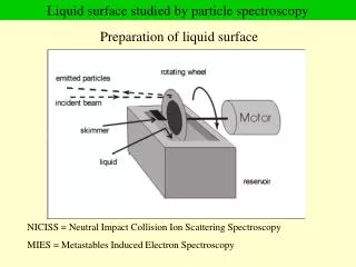
Current Microscopy Example “Advanced Plating Chemistry for 65 nm Copper Interconnects” Semiconductor International May 2003 Mounding when filling trenches with electrochem deposited Cu using two component electrolyte system. No mounding with three component system. Utilized Fast Ion Beam (FIB) Microscope for these images.
Current Spectroscopy Example “Structural Studies in Lithium Insertion into SnO-B2O3 Glasses and Their Applications for All-Solid-State Batteries”, Katada et al., JES 150, A582 (2003) XRD NMR Mössbauer
Ex Situ vs. In Situ Ex Situ Experiment: An experiment performed on a sample after it has been removed from the location wherein it was formed. • wider range of experimental techniques available. In Situ Experiment: An experiment performed on a sample while it is still located in its native environment. • less risk of altering the sample’s true properties.
Remove sample ? Challenges Analyzing Electrochemical Samples Ex Situ • loss of electrochemical control • loss of solvent, ion atmosphere • risk contamination, oxidation
Challenges Analyzing Electrochemical Samples In Situ photons • the electrolyte solution can strongly absorb the various probe particles which might be used to perform different analyses. • cell design needs to account for refraction electrons ions
Red Blood Cells Atoms Viruses 1 Å 1 nm 1 µm 1 mm 1 cm Molecules Computer Circuits Hair Microscopy • What is the structure of the surface of the sample? • Resolution: Lateral, Vertical • Contrast mechanism • Dynamic Range • Ex situ or In situ
1 Å 1 nm 1 µm 1 mm 1 cm Lateral Resolution Here are some of the techniques we will examine and a comparison of their lateral resolution capabilities. AFM OM SAM SEM IM STM
1 Å 1 nm 1 µm 1 mm 1 cm Vertical Resolution Here are the same techniques, comparing their vertical resolution. AFM SAM OM SEM IM STM
OM AFM STM 1 Å 1 nm 1 µm 1 mm 1 cm IM SEM SAM Dynamic Range Not only do we need image small things, but large things too. What is the largest field of view that the instrument can provide? What is the range of features, largest to smallest, that can be observed?
Diffraction vs. Scanning Two approaches to image formation Diffraction: Incident wave scatters from surface features, interfering with itself and forming a diffraction pattern. When diffracted wave is refocused, it produces an image of the surface. •Entire image formed simultaneously •Resolution limited by wavelength Scanning: Incident wave focused to a small point and rastered across surface. Signal is acquired from each point on surface. •Image formed sequentially •Resolution determined by spot size
Vibration Isolation Buildings vibrate (motors, air conditioners, walking, vehicles). Resonances between 1 and 100 Hz. Amplitudes in micron range. • build microscope rigid • couple to building loosely • provide multiple stages with alternate rigid/loose coupling • shield acoustically for very precise measurements
Optical Microscopy • a diffraction experiment • basic lens components • coarse/fine focus • Mon/Bin/Tri ocular schemes • working distance • adjust interpupillary distance • quantitation with reticle • image recording A good web site for a brief introduction to optical microscopes can be found below. http://www.olympusmicro.com/primer/opticalmicroscopy.html http://www.greatscopes.com/important.htm
Optical Microscopy continued Select the correct combination of lenses for your task.
Optical Microscopy Resolution • Rayleigh equation d = 0.61 (l / N.A.) d is distance between objects that can still be distinguished l is wavelength of light N.A. is numerical aperture of lens = n sin(Qvertex) Q
Scanning Electron Microscopy Electron Gun Secondary Electron Detector Vacuum Chamber
SEM Focusing Column Steering Quadrupole 1 Thermal Field Emitter Lens 1 Steering Quadrupole 2 Lens 2 Sample Extractor Beam Acceptance Aperture Deflection Octupole Beam Blanking Plates Suppressor Assembly
SEM Experiment Trochodiscus longispinus in OM and SEM. Note improved depth of field and resolving capability of the SEM experiment.
SEM SEM Electron Reemission Elastically scattered Backscattered e– Inelastically scattered Secondary electron emission Relative Intensity Fraction of Incident Beam Energy
BSE vs. 2° Detection Both can be used, different information, different detection scheme. BSE Specular reflection Higher energy Encode some chemical information 2° Electrons Isotropic emission Very low energy Better structural contrast
X-ray Excitation Depth Profile Incident electron beam penetrates 100 - 200 mm into sample. Different emission mechanisms arise from different depths. BSE SED CL
Atomic Number Dependence The probability of an incident electron being scattered varies as the square of the atomic number of the atom and inversely as the incident kinetic energy. • Greater depth of penetration for low Z materials (e.g. Al vs. W) • BSE emission branch increases with Z Low Z High Z Equation d prop to W V2/Z rho
SEM Example Microstructural Development and Surface Characterization of Electrodeposited Nickel/Yttria Composite Coatings, Cunnane et al., JES 150, C356 (2003) Changing the Y content in the Ni electrolyte bath from 1 to 5 g/L. Preferential growth directions are altered as the nucleation rates are changed by the co-depositing material.
Scanning Auger Microscopy Uses same e-beam source as SEM. Energy analyzes electrons emitted in 100 - 1000 eV range (higher than secondary, lower than backscattered). Provides unique atomic identity information. Very surface specific (10 nm) Chemical maps of surfaces Auger process. Chemical maps. Hemispherical Electron Analyzer. Secondary scattering in samples.
Measure kinetic energy of ejected electron. Incident Electron Beam (5 kV) Another higher level electron is ejected to carry away excess energy. Eject core electron Higher electron falls into hole The Auger Process Vacuum Level M L K Ekinetic = E(K) - E(L) - E(L)
SAM Resolution BS electrons are also scattered into the neighbouring regions of the sample with sufficient energy to further excite atoms not in the original excitation volume. Spatial resolution degraded 2 to 5 times over that of the corresponding SEM resolution.
Scanning Tunneling Microscopy Tunneling gap ~ 5 Å Probe Tip Tunneling Current 10 pA - 10 nA Tunneling Electron Current Sample
Tunneling Mechanism Tip Sample DOS DOS EF VBias EF 0 d IT exp(-2kd)
Density of States Every substance has a complex electronic structure. At every energy, there are a certain number of electronic states. The number is so large for bulk material, that one reports the number of states per unit energy – the Density of States or DOS. Tunneling can occur between states of the same energy; the electron’s energy does not change during the tunneling event.
Control Electronics Feedback Electronics Error Signal Z-piezo Set Point — Difference Current Amplifier Logarithmic Amplifier Sample
R ∆x Resolution Lateral Vertical
In Situ Electrochemical STM There’s still a vacuum gap, even in water! Shield tip to minimize faradaic processes. Melted wax or plastic to coat shank of tip. Expose last few nanometers only. Tunneling current must be large compared to faradaic current.
STM Example #1 Adlayer of 1,10-phenanthroline on Cu(111) in acidic solution Itaya, et al. J.E.S. 150 E266 (2003). Monitored molecular orientation on surface in real time
Scanning Electrochemical Microscope (SECM) http://www.msstate.edu/dept/Chemistry/dow1/secm/secm.html Create an ultramicroelectrode and use the faradaic current as the control signal. Signal modulated by proximity to surface.
Scanning Force Microscopy Depends on forces (repulsive or attractive) between atoms. Diode laser Reflected light To Position Sensitive Detector Sharpened Cantilevered Tip
1+2-(3+4) = 0 1+2-(3+4) < 0 1+2-(3+4) < 0 and 1+3-(2+4) > 0 Position Sensitive Detector 4-Quadrant Photodiode (current in each quadrant changes with light intensity) 2 1 4 3
Contact Mode SFM Repulsive force between surface atoms and tip atoms, lead to cantilever deflection, altering of relected beam path. Sample is rastered and moved vertically to maintain constant cantilever deflection. Can damage delicate samples.
Lateral Force Mode SFM Frictional force measurement. During scan, frictional forces on surface will tend to twist the cantilever. Use Signal = 1+3 - (2+4) as feedback/imaging signal. Chemically sensitive: –CH3 covered surface vs. –COOH covered surface
Non-Contact Mode SFM Important when dealing with delicate samples. Can achieve atomic resolution. Vibrate tip at resonant frequency (100’s of kHz). As tip approaches surface, the attractive forces between the substrate and the tip alter the resonance condition. For feedback/imaging • frequency shift • phase shift • damping
Cantilevers For contact mode For LFM and non-contact mode
SFM Example The Electrochemical Reaction of Lithium with Tin Studied By In Situ AFM, Dahn et al., JES 150, A419 (2003). Li is driven into Sn electrochemically which leads to a swelling of the Sn grains. SFM images were used to measure the grain sizes as the potential changed, contributing to a model rgarding Li incorporation in the Sn film.
Interference Microscopy Visible wavelength optical microscope. Also called Non-contact Profilometry. Nanometer resolution vertical to surface. Uses interferometry to measure surface profile. Large dynamic range. Instrument. Interference technique. Computational process. VSI mode. PSI mode. Angle of acceptance. Terraced surface vs. rough surfaces.
Interference Fringes In-phase reflections are bright; out-of-phase are dark Top view First reflecting surface Structured reflecting surface Side view
Imaging Process Interferometer Recombined, reflected light is directed to image plane of CCD camera. Points on surface that are separated from lens by an integer number of wavelengths is bright; those a half-integer are dark. Objective Lens
Imaging Process continued Interference is strong only when reflected light is in focus; the sample-lens distance is at the focal position. Scan sample-lens distance around the focal length. Each pixel will strongly modulate its intensity when the lens reaches the focal position corresponding to each point on the surface. High resolution position information comes from a linear variable differential transformer (LVDT) connected to the lens scanning drive.
VSI and PSI Modes Vertical Scanning Interferometry Phase Shifting Interferometry Scan objective over range of µm. Record image frames sequentially. Search each pixel through frames and locate frame where intensity modulation is greatest. Assign height information by correlating frame number to LVDT. Alter optical path length in series of steps. This causes fringe pattern to shift laterally. The series of shifted fringe patterns are combined to form interferograms from which height information is calculated
Rough vs. Terraced Surfaces Interference can occur only if light is reflected back into objective lens. If surface angle is inclined beyond acceptance angle of lens, no interference is observed. Lens Angle 2.5x obj. 2° 10x obj. 10° 50x obj. 25° O.K. Missed data Terraced surface
IM Example Preparing Au substrates on mica for use in forming nanostructured electrodes from self-assembled monolayers. Heat treatment created mounds on surface.