Surface Analysis
Surface Analysis. A.) Introduction : Solid Surface: the boundary layer between a solid and either a vacuum, a gas or a liquid - differs substantially in its physical properties and chemical composition

Surface Analysis
E N D
Presentation Transcript
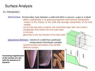
Surface Analysis A.) Introduction: Solid Surface: the boundary layer between a solid and either a vacuum, a gas or a liquid - differs substantially in its physical properties and chemical composition relative to the interior of the solid and average composition of the bulk sample. - not just the top layer of atoms, but a transition layer with non-uniform composition that varies from the outer layer to the bulk. - generally a very tiny fraction of the total solid Operational Definition: volume of a solid that a particular measurement techniques samples - several surface techniques may sample different surface Increasing magnification of the surface of a pin with the presence of bacteria
B.) Spectroscopic Surface Methods: 1. Provide chemical information of the composition of a surface (few D to ~ 10s D thick) To Spectrometer (secondary beam) From source (primary beam) • -Photons, electrons, ions or neutral molecules. • - Need to limit to surface analysis - Results from scattering, sputtering or emission. - Further studied by other spectroscopic techniques Sample Penetration depth of 1-keV electrons is ~ 25 D, where a photon beam of same energy is ~ 104 D
Some Common Types of Spectroscopic Methods for Analysis of Surfaces Methods are differentiated by the nature of the primary and secondary beams
2. Sampling Surfaces and Contamination - focus beam on a single surface - mapping the surface by scanning the beam across the surface in a raster pattern ‚can be linear or two-dimensional ‚observe changes in secondary beam as a function of position - depth profiling etch a hole in the surface by sputtering ‚a finer primary beam is used to generate a secondary beam from the hole ‚observe changes in secondary beam as a function of depth Raster Pattern (data is obtained from primary beam centered in each grid) Depth Profiling
- contamination of the surface from the atmosphere or the primary beam - need to clean surface in vacuum chamber ‚bake sample at high temperatures ‚sputtering the sample with a beam of inert gas ions from electron gun ‚mechanical scraping or polishing the surface with an abrasive ‚ultrasonic washing in various solvents ‚bathing the sample in a reducing atmosphere to remove oxides Surface contamination
3. Electron Spectroscopy - signal from sample is a beam of electrons (secondary beam) - determine the power of the beam as a function of the energy of the electrons (hn) - determine ‚identification of all elements (except H and He) ‚oxidation state of element ‚type of species element is bonded to ‚electronic structure of molecules - poor penetration power of electrons ‚restricted to surface layers of 20 – 50 D -qualitative analysis of the surfaces of metals, alloys, semiconductors and heterogeneous catalysts Different element abundance in different regions of the surface
A). Electron Photoelectron Spectroscopy (XPS) i.Theory - record kinetic energy of emitted electron ‚plot of number of emitted electrons as a function of the energy of the emitted electron - X-ray beam of known energy (hn) displaces an electron A + hn A+* + e- -Kinetic energy of emitted electron (Ek) is measured in an electron spectrometer ‚Binding energy (Eb) of the electron is: Eb = hn - Ek - w where: hn – energy of electron beam Ek – measured kinetic energy of emitted electron w – work function of spectrometer (determined experimentally) Photoelectric Process
- well separated peaks for each element on the surface can be observed ‚except hydrogen - observe multiple peaks for each element ‚S, P and D orbital ‚energy decreases as a function of orbital S > P > D ‚energy increases as a function of atomic number N1s > C1S Binding Energy of an electron is characteristic of the atom and the orbital from which the electron was emitted Binding Energy (eV)
Computer System Hemispherical Energy Analyzer Outer Sphere Magnetic Shield Analyzer Control Inner Sphere Multi-Channel Plate Electron Multiplier Lenses for Energy Adjustment (Retardation) Resistive Anode Encoder X-ray Source Position Computer Lenses for Analysis Area Definition Position Address Converter Position Sensitive Detector (PSD) Sample ii.Instrumentation - Expensive ($300,000 - $900,000) - Requires extensive vacuum systems (10-5 to 10-10 torr) - Similar to optical spectrometers
- X-ray source (X-ray tube) ‚bombardment of a metal target with a beam of high-energy electrons - electrons produced at heated cathode - accelerated to metal anode, copper block with target (Mg, Al) - large potential (100 kV) ‚X-rays produced by decelerated electrons upon collision with target - energy of photon is equal to the difference in kinetic energy of the electron before and after collision. - deceleration occurs as a series of collisions different kinetic energy losses - X-ray energies vary over a continuum ‚Very inefficient, less than 1% of electrical power converted to X-rays - remainder dissipated as heat - water cooling is required
- Sample holders ‚samples mounted as close to X-ray source as possible - avoid attenuation of X-ray ‚sample container under a vacuum (<10-5 torr, typically 10-9 to 10-10 torr) - avoid contamination of sample surface by water or oxygen - avoid attenuation of X-ray beam due to inelastic collisions - Analyzers ‚hemispherical type ‚electron beam deflected by an electrostatic magnet - electrons travel in a curved path - radius of curvature is dependent on kinetic energy of electron - vary field, direct electrons of different kinetic energy onto detector. ‚ under a vacuum (<10-5 torr) - Transducer (detector) ‚solid-state, channel electron multipliers ‚tubes of glass doped with lead or vanadium - apply a potential of several kilovolts across these materials - a cascade of electrons (106 -108) for each incident electron - pulses are counted electronically ‚similar in concept to photomultiplier tubes
iii.Chemical Shifts and Oxidation States - position of a peak is dependent on the chemical environment of the atom - variations in the number of valence electrons and type of bond influence the binding energy of the core electrons Binding energy increases as a function of electronegativity Similar effects observed for different Oxidation states
Similar effects observed for different Oxidation states Electron volts relative to oxidation state marked by *
B). Auger Electron Spectroscopy (AES) i.Theory - two-step process, generates Auger electron ‚differs from XPS 1) generate excited ion as before: A + hn A+* + e- or using an electron beam A + ei- A+* + ei’- + eA- where: ei’- is the beam electron after interaction with A and loss of kinetic energy. eA- is ejected from A inner orbital 2)excited ion may relax by emitting an Auger electron (eA-) with kinetic energy (Ek) A+* A++ + eA- or by fluorescence (X-ray fluorescence) A+* A+ + hnf -Kinetic energy of emitted electron (Ek) is independent of the energy of photon or electron that ‚Kinetic energy (EK) of the Auger electron is: EK = (Eb – Eb’) – E’b = Eb – 2Eb’ where: (Eb-Eb’) – energy released in relaxation of the excited ion Eb’ – energy required to remove the second electron from its orbit
- Auger emissions are described in terms of the type of orbital transitions involved in the production of an electron ‚KLL: 1. removes a K electron 2. transition of an L electron to the K orbital 3. ejection of a second L electron ‚LMM and MNN are also common transition - measurement of the kinetic energies of the emitted electrons ‚each element in a sample being studied will give rise to a characteristic spectrum of peaks at various kinetic energies. ‚Spectra typically displayed as a derivative (dN(E)/dE) - enhance small peaks, repress effects of intense peaks - Auger electron emission and X-ray fluorescence are competitive processes ‚lower atomic number Auger electron emission ‚higher atomic number X-ray fluorescence AES Sample: Pd Ep = 2.5 Kev
ii.Advantages • - sensitivity to atoms of low atomic number • - minimal matrix effects • - high spatial resolution • ‚detailed examination of solid surfaces • ‚electron beam more tightly focused than X-ray beam • iii. Disadvantages • - not used to provide structural and oxidative state information (XPS) • - quantitative analysis is difficult • iv. Instrumentation • - similar to XPS, most instruments do both XPS and AES • - requires an electron gun
Diagram of Electron Gun • Heated tungsten filament • 0.1 mm diameter • Bent into shape of hairpin with V- • shaped tip • maintained at potential of 1 -50 kV • Wehnelt cylinder • surrounds filament • negative bias to filament (0-3000V) • electric field of Gun causes electrons to • converge at crossover • Produces a beam of electrons of 1 to 10 keV • can be focused onto the surface with diameters of 500 to 5 mm
4. Scanning Electron Microscopy - high resolution images of surfaces ‚optical microscopy limited by wavelength of light, diffraction effects - surface is swept in raster pattern with finely focused beam of electrons ‚swept in straight line in x-direction ‚returned to starting point ‚shifted downward (y direction) by a standard direction Cecropia Moth Scales (15,000x) Cecropia Moth Scales (350x)
A). Scanning Electron Microscope (SEM) i.Introduction - surface is scanned with beam of electrons - several types of signals from the surface are created ‚backscattered or secondary electrons - two most common for SEM ‚X-ray fluorescence ‚Auger electrons • -Condensing lens and objective lens reduce electron beam to final spot of 5 to 200 nm • Two magnet coils in objective lens deflect e- beam in x and y direction to scan surface • intensity of beam created from surface are used to drive the horizontal and vertical scans of a cathode-ray tube (CRT). • Magnification (M) = W/w • where: • W – width of CRT • w – width of single line • scan across the sample
- increased magnification is achieved by decreasing w ‚narrower the beam of electrons the higher the magnification ‚magnification range is 10x to 100,000x Increasing Magnification of Mosquito - samples changers are designed for rapid changing of samples ‚large-capacity vacuum pumps bring pressure to < 10-4 torr ‚can hold samples many centimeters in length ‚can be moved in x, y and z directions - sample considerations ‚samples that can conduct electricity are easiest to study - flow of electrons to ground minimize artifacts - also typically good conductors of heat - minimize thermal degradation ‚most biological and mineral samples do not conduct electricity - coat surface with thin metallic film by sputtering or vacuum evaporation - detectors ‚scintillation device - doped glass or plastic emits photons when struck by electrons
- detectors ‚scintillation device - doped glass or plastic emits photons when struck by electrons - photons conducted by light tube to photomultiplier tube (outside instrument) - gains in signal of 105 to 106 ii.Interaction of Electron Beams with Surface - elastic interactions ‚affect the trajectory of electron not energy ‚deflection of collision is random (0 to 180 deg.) ‚beam penetrates to a depth of 1.5 mm or more ‚eventually exit from surface as backscattered electrons - larger diameter limits resolution - inelastic interactions ‚transfer part or all of energy from electron to solid ‚excited solid emits secondary electrons, Auger electrons, X-rays Simulation of Electron Trajectories
- Secondary Electron Production ‚electrons having energies of 50 keV or less are emitted from surface - along with backscattered electrons - ½ to 1/5 number of backscattered electrons ‚beam ejects conduction band electrons ‚only from depth of 50 to 500 D ‚slightly larger beam than incident beam ‚prevent from reaching transducer by a small negative bias - X-ray emission ‚characteristic line spectra and continuum are produced • (1) column hosts the electron beam. • (2) microscope is operated from the steering panel • (3) cryo-unit with a binocular • exchange chamber is used to introduce the object into the high vacuum area. • The object can be observed on the large screen while it is scanned. • The small screen serves to watch the object chamber. • The computer for image archiving and processing. • electronics
5. Scanning Probe Microscopes - resolve details of surface to the atomic level ‚Nobel Prize in 1986 fro G. Binnig and H. Roher - provides details in x, y and z dimension ‚20 D resolution in x, y as low as 1 D ‚resolution in z better than 1 D ‚electron microscope resolution is 50 D direct observation of standing-wave patterns in the local density of states of the Cu(111) surface. These spatial oscillations are quantum-mechanical interference patterns caused by scattering of the two-dimensional electron gas off the Fe atoms and point defects.
A). Scanning Tunneling Microscope i.Introduction - surface must conduct electricity - surface is scanned in raster pattern with a very fine metallic tip - tip is maintained at constant distance from sample by maintaining a constant tunneling current ‚up and down motion of tip reflects topology of surface ‚tunneling current created by voltage between tip and sample Constant (d) V Scanned graphite surface STM tip scanning graphite surface (spheres are carbon atoms)
ii.Tunneling current - current that passes through a medium that contains no electrons ‚vacuum, nonpolar liquid, aqueous electrolyte solution ‚explained by quantum mechanics - tunneling currents become significant when ‚two conductors are within a few nanometers of each other ‚one conductor is in the form of a sharp tip - tunneling current (It) is given by: It = Ve-Cd where: V – voltage between conductors C – constant dependent on composition of conductors d – spacing between tip and surface - tunneling current is held by moving tip up and down so d is constant ‚tip is moved by potential change in x, y or z dimension that causes a hollow-tude piezoelectric device to bend in the x,y plane or extend/shrink along z-axis Image of STM Tip The inner and outer curved surfaces are coated with a thin metal layer to form two electrodes. The piezo tube bends under application of unequal voltages to the electrodes. Accuracy of movement is on the order of 1 nm
iii.Tips - critical to performance of SEM - best images when the end of the tip is a single metal atom ‚tunneling current increases by 10x when gap distance decreases by 1 D ‚all current flows to single atom that is 1 D closer to surface than all other atoms - tips constructed by: ‚cutting platinum/iridium wires ‚electrochemical etching of tungsten metal ‚exponential increase in tunneling current with decreasing gap makes it possible to prepare single atom tip Image of STM Tip SEM used to move Fe atoms
B). Atomic Force Microscope (AFM) i.Introduction - resolution of individual atoms on both conducting and insulating surfaces ‚STM requires conducting surface - flexible force-sensing cantilever stylus is scanned over the surface - force acting between cantilever and surface causes minute deflections of the cantilever ‚deflections detected by optical means ‚motion of cantilever controlled by piezoelectric tube (same as STM) 1. Laser 2. Mirror 3. Photodetector 4. Amplifier 5. Register 6. Sample 7. Probe 8. Cantilever Bending or tapping of cantilever as it moves across service Images of cantilever and tip
- laser beam is reflected off a spot on the cantilever to photodiode that detects the motion ‚output from phtodiode then controls force on cantilever - output from photodiode then controls force on cantilever so that it remains constant ‚similar to tunneling current control in STM ‚motion of cantilever controlled by piezoelectric tube (same as STM) • ii.Tips and Cantilever • - critical to performance of AFM • - originally crushed diamonds attached to metal foil • - currently, tips constructed by: • ‚etching single chips of silicon, silicon oxide or silicon nitride • ‚remarkably small and delicate • -few tens of mm in length, less then 10 mm in width, ~ 1 mm • thickness • - tips are few mm in height and width Can view cantilever as coil spring
iii.Tapping Mode Operation • - disadvantages of contact mode scanning • ‚potential damage of surface and distortion of image • ‚especially problematic with “soft” samples • -biological samples • - polymers • - silicon wafers • - Tapping mode • ‚only allow tip to contact surface briefly then removed from surface • ‚cantilever oscillates at frequency of few 100 kHz • ‚image material that was impossible to image by contact mode Atomic force microscopy images of reconstituted nucleosomal arrays. (A) A chromatin fiber with a beads-on-a-string morphology reconstituted at 1 : 1 histone octamers to DNA ratio. (B) When 1.5 : 1 histone octamers to DNA ratio is used for reconstitution a condensation of the core histone octamers is observed