Download
1 / 36
580 likes | 1.89k Vues
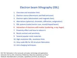
Electron beam lithography (EBL). Overview and resolution limit. Electron source (thermionic and field emission). Electron optics (electrostatic and magnetic lens). Aberrations (spherical, chromatic, diffraction, astigmation). EBL systems (raster/vector scan, round/shaped beam)

E N D
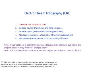
Electron beam lithography (EBL) Overview and resolution limit. Electron source (thermionic and field emission). Electron optics (electrostatic and magnetic lens). Aberrations (spherical, chromatic, diffraction, astigmation). EBL systems (raster/vector scan, round/shaped beam) Interaction of electrons with matter (scattering, x-ray, Auger). Proximity effect and how to reduce it. Resist contrast and sensitivity. Several popular resist materials. High resolution EBL, resolution limit. Grey-scale EBL for 3D structure fabrication. Anti-charging techniques. Electron projection and multi-beam lithography ECE 730: Fabrication in the nanoscale: principles, technology and applications Instructor: Bo Cui, ECE, University of Waterloo; http://ece.uwaterloo.ca/~bcui/ Textbook: Nanofabrication: principles, capabilities and limits, by Zheng Cui
Resolution enhancement process: ultrasonic development Ultrasonic helps to remove exposed resist (for positive tone) from inside narrow trenches.
Resolution enhancement process: low temperature development (ZEP) Contrast curve for ZEP-520 at various temperatures Contrast as a function of development temperature. Comparison of edge roughness of ZEP-520 resist lines (40nm wide) developed at (top) room temperature; (bottom) -4oC. Low T development increases contrast, but decreases sensitivity
Resolution enhancement process: low temperature development (PMMA) Figure 2-6: Schematic illustration of one possible explanation of resolution-enhancing mechanism of cold development. When a feature is exposed in PMMA, the soluble resist in the exposed region is surrounded by a boundary region of resist that, due to the initial polydispersity of the PMMA and random nature of chain scission, contains both soluble and insoluble polymer chains. During development, this region phase-separates, with the soluble chains diffusing toward the soluble region and the insoluble chains diffusing toward the insoluble region. The result is a region of soluble PMMA that is larger than the initial exposed feature, resulting in a degradation in resolution. Cold development helps prevent this by limiting the diffusion that can occur in the boundary region, since diffusion is a thermally-dependent process. The exact mechanism of cold development is still not clear. Another possible mechanism: colder developer is weaker solvent, so less attack to unexposed or partly exposed resists. PhD thesis, Bryan M. Cord, MIT, June 2009
Cold (to -60oC) development of PMMA Best contrast (steepest slope) at -15oC. Because, at even lower temperature, need higher dose to expose, but PMMA becomes negative at doses >3000 C/cm2(i.e. the already exposed PMMA with short chain begins to cross-link upon further exposure). Figure 2-10: Measured contrast curves for PMMA developed in 3:1 IPA:MIBK at various temperatures. The initial resist film thickness was 160 nm and the development time was 60 seconds, except in the -40°C and -50°C cases (120 seconds) and the -60°C case (600 seconds), where longer development times were needed to show any measurable dissolution at all. IPA: iso-propanol; MIBK: methyl isobutyl ketone PhD thesis, Bryan M. Cord, MIT, June 2009
Forward scattering α: forward scattering range, with unit nm Figure 3-5: Forward scattering coefficients as a function of beam energy for various thicknesses of PMMA, calculated using CASINO, a free Monte Carlo modeling program. The forwarding scattering width decreases dramatically as the beam energy is increased, but using thicker resist results in more scattering. PhD thesis, Bryan M. Cord, MIT, June 2009
Why weaker forward scattering at higher energy Incident/primary electron For simplicity, assume the electric field from the secondary electron acted on the primary electron is uniform covering a distance d. Forward scattering: deflect primary electron, generate secondary electron to expose the resist - - Secondary electron x - d E z Higher energy, larger Vz, so smaller Vx. V: velocity P: momentum A: acceleration) resist
Resolution limit: forward scattering and lateral diffusion Figure 3-6: Schematic illustration of secondary electrons (SE), which typically travel/diffuse normal to the beam. (low energy SE is responsible for resist exposure) Secondary electrons and its lateral diffusion Backscattered electron Backscattered electron Forward-scattered electron Whether it is forward scattering or beam spot size that limits the minimum line-width, the effect of SE diffusion is to further broaden the line/reduce the resolution.
Resolution limit: forward scattering and beam diameter Figure 3-19: Beam diameter as a function of beam energy as measured in the MIT Raith-150 system. While beam diameter is inexplicably large at voltages below 10kV, it seems to be reasonably close to its 3-4 nm specification at higher kV, suggesting that beam diameter is not the limiting factor in the resolution (see next slide). Figure 3-11: “Critical thickness” of resist as a function of beam energy. At resist thicknesses above critical thickness, forward scattering limits resolution, whereas below the critical thickness the only resolution limiter is the beam diameter, which is at least theoretically energy-independent. A third limiting factor is resist swelling by developer. PhD thesis, Bryan M. Cord, MIT, June 2009
The highest resolution by far: 9nm pitch grating Backscattering/proximity effect is not important here, since pattern area only 50nm. For large area (>>1m) grating, such a small pitch may not be achieved due to proximity effect. Here resist very thin, 25nm. Figure 3-20: 9-nm-pitch nested-L structure fabricated in HSQ on Si and imaged in the MIT Raith-150 system (left) and on the Raith-150TWO prototype tool. The left image shows minimal to nonexistent modulation, while the discrete lines of the structure are clearly visible in the right image, possibly due to the much better vibration isolation. PMMA should have similar or even better resolution, but difficult to image (too soft, whereas exposed HSQ is rigid SiO2 without deformation during imaging), PMMA doesn’t stick to substrate well (may be lifted off during development), and lines may fall due to capillary force during drying after development. PhD thesis, Bryan M. Cord, MIT, June 2009
Electron beam lithography (EBL) Overview and resolution limit. Electron source (thermionic and field emission). Electron optics (electrostatic and magnetic lens). Aberrations (spherical, chromatic, diffraction, astigmation). EBL systems (raster/vector scan, round/shaped beam) Interaction of electrons with matter (scattering, x-ray, Auger). Proximity effect and how to reduce it. Resist contrast and sensitivity. Several popular resist materials. High resolution EBL, resolution limit. Grey-scale EBL for 3D structure fabrication. Anti-charging techniques.
Gray-scale electron beam lithography AFM of a grating in resist E-beam exposure with variable doses to create variable depths after development. 5m RIE pattern transfer into Si PMMA Silicon Fresnel zone lens (plate) in silicon
Which resist is best for gray-scale EBL? Negative tone PES Contrast curve of PES with 10keV electron beam. Sensitivity was found to be 200C/cm2, with contrast only 0.8. Contrast curve of PMMA • Ideal resist has positive tone with very low contrast (ideally <1) and high sensitivity. • High contrast leads to very narrow process/dose window (tiny dose change large pattern depth change). • When using negative resist, make sure that the electrons can reach resist bottom (otherwise, resist at bottom will be dissolved by developer, lifting off all the resist above). Bryce, “Poly(ether sulfone) as a negative resist for electron beam lithography”, APL, 90, 203110 (2007).
Micro and nano optical elements in silicon and silica by regular and gray scale e-beam lithography
Electron beam lithography (EBL) Overview and resolution limit. Electron source (thermionic and field emission). Electron optics (electrostatic and magnetic lens). Aberrations (spherical, chromatic, diffraction, astigmation). EBL systems (raster/vector scan, round/shaped beam) Interaction of electrons with matter (scattering, x-ray, Auger). Proximity effect and how to reduce it. Resist contrast and sensitivity. Several popular resist materials. High resolution EBL, resolution limit. Grey-scale EBL for 3D structure fabrication. Anti-charging techniques.
Charging during e-beam writing • Even though most resists are insulating, charging is not an issue for typical resist thickness of <500nm, because most electrons penetrate deep into the conducting substrate at 30kV. (more serious charging for lower kV) • When electron beam lithography must be performed on insulating substrates (quartz, SiO2/Si…), negative charge buildup can occur on substrate surface, causing beam deflection, and thus pattern distortion. Future Condition Initial Condition electron beam electron beam repulsive electric potential lines ma-N 2403 negative resist Glass substrate negative charge accumulation
Anti-charging technique: coat conducting layer • To eliminate charging effect, one can coat a conducting layer on top of or beneath the resist. • Typically 10nm metal is enough, such as Al, Ti, Cr or Au; conducting polymer may also work. • Lighter metal (Al) causes less (forward) scattering of electron beam than the heavier one (Au), so is preferred. • Al and Ti can be removed easily by diluted HF (1:100 diluted). • Some resist (such as SU-8) is sensitive to UV/x-ray light generated during e-beam (10keV beam energy) evaporation of the metals (thermal evaporation or sputtering is OK). BAD (severe charging) GOOD (no charging) no anti-charging layer Coat metal
Anti-charging technique: variable pressure (VP) EBL • It is the same idea as VP-SEM, i.e. introducing gas (H2O, N2, Ar, He) into the chamber. • Gas molecules are ionized by electron impact; these positive gas ions migrate to negatively charged surface and balance surface charge. • Primary electron beam will be scattered to some extent by collision with gas molecules, forming a beam “skirt” around the focused primary beam at sample surface. • Higher energy e-beam has less “skirt”; butit is shown that “skirt” doesn’t noticeably reduce resolution. • (For SEM only) Gas also amplifies secondary electron (SE) signal by “gas cascade” effect. VP-SEM images of a pattern on glass substrate with 30keV e-beam writing under high vacuum 0.4 Torr (water vapor pressure) 1 Torr The dashed red line indicates the pattern dimension as written. The pattern exposed with 1Torr pressure shows no significant distortion or displacement. “Variable pressure electron beam lithography (vp-ebl): A new tool for direct patterning of nanometer-scale features on substrates with low electrical conductivity”, Nano Lett. 6(5), 963-968(2006).
Anti-charging technique: critical energy EBL How to find E2? Reduce magnification, here from 500× to 200× at acceleration voltage: 0.5keV 1.3 keV 2.0 keV Electron accumulated during imaging at 500×. When zoom out to 200×, more electrons ejected at the charged region, so is brighter. Total (ejected) electron yield (σ) vs beam energy for a typical resist. positively charged Negative charge Positive charge Virtually no charge negatively charged • Bulk insulating material is positive charged when σ > 1 and negatively charged when σ < 1. Charge buildup is zero at critical energy/crossover voltage (E1, E2), where σ is unity. • In between, >1, so >1 electron (including SE and BSE) ejected for each incident electron. • E1 is too small, E2 depends on resist thickness and substrate material. • For 65nm PMMA on glass, E2=1.3keV. Such low keV can penetrate such thin resist. “Nanoscale Patterning on Insulating Substrates by Critical Energy Electron Beam Lithography”, Nano Lett. 6(9), 2021-2025 (2006).
Anti-charging technique: critical energy EBL No deflection at 1.3keV Result of EBL writing 100nm Line deflection determined by SEM measurement at various voltages based on methods reported by Craighead. (Two parallel single-pass reference lines were first patterned with a 1μm gap, followed by charge pads written at 30μC/cm2. Finally, a third single-pass line was patterned between the pad and the reference line) SEM images of 5nm thick Au after lift-off. The minimum feature size was 60nm with an area dose 10μC/cm2 (PMMA resist). Low voltage difficult to get high resolution, here only 60nm. But the sensitivity becomes very high, only 10C/cm2, (250C/cm2 for 30kV).
Electron beam lithography (EBL) Overview and resolution limit. Electron source (thermionic and field emission). Electron optics (electrostatic and magnetic lens). Aberrations (spherical, chromatic, diffraction, astigmation). EBL systems (raster/vector scan, round/shaped beam) Interaction of electrons with matter (scattering, x-ray, Auger). Proximity effect and how to reduce it. Resist contrast and sensitivity. Several popular resist materials. High resolution EBL, resolution limit. Grey-scale EBL for 3D structure fabrication. Anti-charging techniques. Electron projection and multi-beam lithography
High throughput electron-based lithography: overview • Electron beam lithography using single beam is too slow for mass production. • Three directions to increase throughput drastically: • Use broad beam and mask, like photolithography. It is called electron projection lithography (EPL), with SCALPEL as best known EPL method. • Start from a broad beam, divide into many sub-beams, like zone-plate x-ray lithography. • Using an array of mini-electron guns/sources to generate multi-electron beams. • Those techniques can also be used for ion, will be addressed later. • Currently, multi-e-beam direct write is competing with EUV lithography for next generation lithography.
ITRS (2006) Projections for Lithography Technology ML2: mask-less lithography - EBL, SPM (scanning probe microscope) tip based lithography..
MEMS-based electron emitters array Not mature, far away from mass production tool. Same principle as field emission display, go to see http://en.wikipedia.org/wiki/Field_emission_display
SCALPEL: Scattering with angular limitation projection electron beam lithography Dark and light regions differentiated by their scattering strength at the SCALPEL aperture. Harriott, JVST B, 15(6), 2130-2135 (1997)
SCALPEL: mask • Mask is like that for x-ray lithography, consisting of membrane and “absorber”, which are both almost completely electron-transparent at 100keV electron energy. • This means that very little of the incident energy is actually absorbed by the mask, minimizing thermal instabilities in the mask. • Si3N4 membrane with thickness order 100nm; “absorber” typically W. • Such a membrane mask is nothing robust. As a result, like x-ray lithography, mask problems make electron projection lithography unsuitable for mass production, despite the great investment the semiconductor tool company has put in it. World first 200mm mask fabricated by HOYA
Coulomb interaction between electrons limit resolution Coulomb repulsion is important because all electrons not scattered by “absorber” pass the small aperture where the current density/repulsion is highest. resolution (the current that passed through the aperture)
SCALPEL summary • Electron energy 100keV, negligible diffraction. • Reduction is possible, such as 4 (i.e. pattern on mask 4 that on resist). • Target resist sensitivity is <5C/cm2, which is over 100 faster than PMMA. • Shot noise and line-edge-roughness would be an issue. • Up to around year 2000, EPL had been considered as a promising next generation lithography to replace photolithography, but no more for today, partly because its resolution is no longer impressive. • Problems: • Alignment method. • Pattern distortion/resolution limit due to repulsive force among electrons. 60nm line/space pattern by EPL Resist development Positive Negative
Projection Mask-Less Patterning (PMLP) In principle, can also be electron source In Vienna
MAPPER system At present, MAPPER system seems to be the most promising multi-beam direct write system. (IMS at Vienna described in previous slides focused more on ion beam lithography) A few demo-tools have been shipped to semiconductor industry. Raster scan, beam blanker by optical control For the video, see http://www.mapperlithography.com/technology.html
Most recent views (NGL: next generation lithography) Abstract: A comparison of ArF immersion single exposure, double patterning, extreme UV, and multi-e-beam maskless lithography (MEB ML2) systems, is made on their special characteristics, then in footprint, cost, and raw energy consumption. Only the MEB ML2 system has the potential to mimic ArF immersion single exposure in the three areas compared. In addition, MEB ML2 does not have the burden of mask-contributed CD and overlay variation, mask cost, cycle time, pellicle, contamination, and electrostatic-discharge-induced damage. Key challenges to develop MEB ML2 into a high-volume manufacturing technology are also given.
Most recent views Footprint “Despite the tremendous potential of MEB ML2, it has the least momentum in NGL. Perhaps its conception is way after much investment is made in other NGL such as EUV lithography, even after the ill attempt of e-beam projection printing (i.e. electron projection lithography) which experienced insurmountable mask problems amongst other obstacles. The latter leaves bad taste with e-beam technology while the former consumes development funds too large to abandon.” • Multi-electron beam (MEB) writing has smallest footprint. So within the same footprint as EUV, one can put 10 MEB systems, in order to gain similar throughput (100 wafers/hour). • MEB doesn’t need the rather expensive masks, the tool is also less expensive. • The main extra cost for MEB is high data rate and expensive data handling hardware. • Each writing field contains 20TBytes. Data rate 4Gbits/sec means CMOS beam blanker with even higher rate is needed. ML2=MLL=mask-less lithography; NGL=next generation lithography