Download
1 / 1
10 likes | 249 Vues
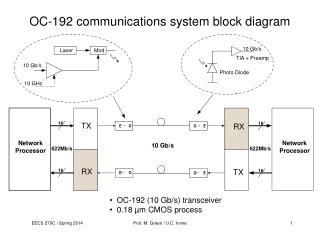
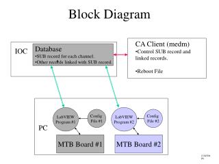
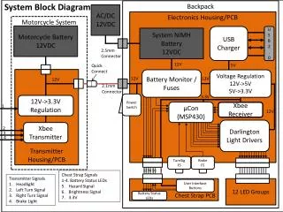
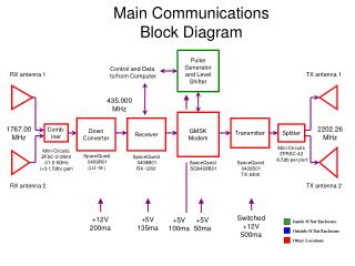
Main Communications Block Diagram. Pulse Generator and Level Shifter. Control and Data to/from Computer. RX antenna 1. TX antenna 1. 435.000 MHz. GMSK Modem. Down Converter. Receiver. Transmitter. 1767.00 MHz. 2202.26 MHz. Comb- iner. Splitter. Mini-Circuits ZFRSC-42

E N D
Main CommunicationsBlock Diagram PulseGeneratorand Level Shifter Control and Data to/from Computer RX antenna 1 TX antenna 1 435.000MHz GMSKModem DownConverter Receiver Transmitter 1767.00MHz 2202.26MHz Comb-iner Splitter Mini-Circuits ZFRSC-42 -6.5db per port Mini-Circuits ZFSC-2-2500 .01-2.5GHz (+3-1.5db) gain SpaceQuest 0409R01(LU-18 ) SpaceQuest 0408B01RX-1200 SpaceQuest SQ0408B01 SpaceQuest 0409S01TX-2400 RX antenna 2 TX antenna 2 Switched +12V 500ma +12V 200ma +5V 135ma +5V 100ma +5V 50ma Inside ICSat Enclosure Outside ICSat Enclosure Other Locations