RF Amplifier for EOM Modulation with Splitter and Attenuators
A detailed plan for an RF amplifier designed for driving Electro-Optic Modulators, featuring a 2-way splitter, attenuators for modulation depth tuning, and potential bandpass filters. Includes chassis designs for different frequencies.

RF Amplifier for EOM Modulation with Splitter and Attenuators
E N D
Presentation Transcript
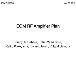
JGW-T1809211 Jan 28, 2018 EOM RF Amplifier Plan Tomoyuki Uehara, Kohei Yamamoto, Keiko Kokeyama, Kiwamu Izumi, Yuta Michimura
Summary • RF Amplifier for driving EOM • Basically same as RF Distribution Amplifier (JGW-D1706462) - But 2-way splitter instead of 8-way - Include some attenuators to tune modulation depth (could be voltage controlled one) - Might include some bandpass filters - Different front panel, same rear panel • Make at least 3 chassis for f1,f2,f3 - f1: 16.881 MHz (split into two) - f2: 45.016 MHz (no split) - f3: 56.270 MHz (split into two) • RF parts will be prepared and assembled by MIF/IOO
Top Assembly Plan JGW-D1706462 Rear panel same as JGW-D1706468 Some attenuators in between Two way splitter (not 8-way) Front panel plan in next page
Front Panel and RF Chain Attenuators will be put outside of the chassis during commissioning period for easier tuning ZFSC-2-1-S+ • Design available at JGW-D1809208 • Rear panel same asJGW-D1706468 ZX30-20-4 wil be voltage controlled in the future RF monitor LNBA-11-23-CK VAT-3+ VAT-3+ attenuation level depends on mod freq. (see p.5) VAT-?+ VAT-?+ RF input (N) Two RF outputs (N) Two voltage inputs for voltage controlled attenuators (BNC) *We might want to isolate this connector from chassis
Parts Prepared by MIF/IOO • U1: RF amplifier Wenzel LNBA-11-23-CK-100-15(in hand) • U2: RF coupler Mini Circuits ZX30-20-4 (in hand) • U3: two-way RF splitter Mini Circuits ZFSC-2-1-S+ (ordered) • RF attenuators (Mini Circuits VAT-1+ etc) (ordered) • Voltage controlled RF attenuators (Teledyne GC2510 ?) (ordered) • Bandbass filters (TBD, if necessary) • TO BE DISCUSSED - Mounting plate? (like JGW-D1706464) - Connectors and cables(semi-rigid SMA cables)?
Variations • f1: 16.880962 MHz in -> amplifier -> splitter -> -3dB (variable) -> -4dB -> out -> -3dB (variable) -> -3dB -> out • f2: 45.015898 MHz in -> amplifier -> splitter -> -3dB (variable) -> (-5dB) -> out • f3: 56.269873 MHz in -> amplifier -> splitter -> -3dB (variable) -> -6dB -> out -> -3dB (variable) -> -7dB -> out “-3dB (variable) ” are the ones which will be replaced to voltage controlled attenuators in the future (-5dB attenuator for if no MZM)