Download
1 / 13
130 likes | 256 Vues
This paper presents the design of a fully digital data acquisition module for positron emission tomography (PET) scanners, emphasizing high energy and timing resolution, as well as high count rate capability. Using advanced FPGA technology and time-of-flight (TOF) information, the system offers enhanced image reconstruction compared to traditional PET methods. The implementation involves optimized digital signal processing techniques, ensuring optimal performance regarding energy and timing resolutions while managing throughput. Key challenges and solutions in achieving these performance standards are discussed, alongside the system's experimental setup and evaluation.

E N D
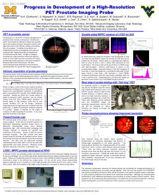
A flexible FGPA based Data Acquisition Module for a High Resolution PET Camera Abdelkader Bousselham, Attila Hidvégi , Clyde Robson, Peter Ojala and Christian Bohm
Objective ? • To design a fully digital data acquisition module for a positron emission tomography Scanner (PET) with: 1- High energy resolution 2- High timing resolution 3- High count rate
Time of flight ? • The faster decay time and higher light output of LSO crystal excellent timing resolution ( 300 ps ) • Using time of flight (TOF) information in PET provide a better reconstructed image than conventional PET t1 t2
Challenges • How to obtain an optimal performance with respect to energy, time resolution and throughput simultanously Free running ADC and Digital signal processing with Optimal Filtering
c 2 A vector of N samples of the pulse The weight function for the three parameters Optimal filtering • it can be derived from weighted least squares or fits of a reference pulse to a sampled pulse • it gives the maximum likelihood estimator of the amplitude and time if the noise is stationary and Gaussian Time Base line Amplitude Inverse of noise covariance matrix
Algorithm for digital implementation We calculate and tabulate for the amplitude Observing the outcome of the scalar product for different times and searching for a maximum amplitude. The amplitude and time can be obtained by interpolation using a 2nd degree polynomial. where Since if is the maximum, the zero crossing of Can be used to find the peak. And
Digital signal processing with free running ADC • Schematic representation of the exprimental setup Digital signal processor Signal from detector ADC High speed serial link Monitoring and controlling PC
The two solutions DSP - Digital Signal Processor - Specialized for digital signal processing. - Well suited for FIR filter type calculation. - Easy to program - But limited in performance by clock rate.
The two solutions • FPGA - Field Progammable Gate Array • Allows massive parallelism • Today: programmable FPGAs have high performance for digital signal processing • Dedicated DSP blocks (MAC, BRAM, DCM). • IP cores for DSP. • Processors and Busses (PowerPC, MicroBlaze..,OPB, PLB..) • Result: “Systems on programmable Chips”. + sea of gates.
OPB_BUS MAC MAC_Array Logic_conroller BRAM Addr. Cntr. MAC_Aray MAC_BLOCK FIFO MAC_Block_3 MAC_Block_2 Pipeline Memory Y30 Y31 Y32........Y3N X30 x31 x32........x3N 3 2 1 0 -1 -2 -3 3 2 1 0 -1 -2 -3 Y20 Y21 Y22........Y2N X20 x21 x22........x2N Y10 Y11 Y12........Y1N X10 x11 x12........x1N Y00 Y01 Y02........Y0N X00 x01 x02........x0N X-10 x-11 x-12........x-1N Y-10 Y-11 Y-12........Y-1N Y-20 Y-21 Y-22........Y-2N X-20 x-21 x-22........x-2N X-30 x-31 x-32........x-3N Y-30 Y-31 Y-32........Y-3N Implementation Binary search Data from ADC N Mac blocks MAC_Block_A Trigger Logic MAC_Block_1 Amp_Time Calculation Zero_Crossing Energy Enable OPB_Bus MicroBlaze Xilinx FPGA
Pipeline Memory Network PC for control and monotoring Initialisation and Calibration Data from ADC Trigger Logic FIFO Pulse_processing Enable MicroC/OS-II on MicroBlaze Xilinx_FPGA
Summary Critical components have been tested • High speed ADCs using evaluation board. • Pulse processing using commercial SP board • Embeded processor implementation using Virtex2 Pro board. • Embeded pulse processing implementation using simulations Remains system integration using Virtex4 FPGA