Download
1 / 33
380 likes | 663 Vues
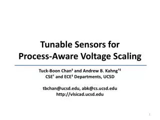
Tunable Sensors for Process-Aware Voltage Scaling. Tuck-Boon Chan ‡ and Andrew B. Kahng † ‡ CSE † and ECE ‡ Departments, UCSD tbchan@ucsd.edu , abk@ cs.ucsd.edu http:// vlsicad.ucsd.edu. Outline. Intro: Adaptive Voltage Scaling (AVS) Overview of Proposed Method

E N D
Tunable Sensors for Process-Aware Voltage Scaling Tuck-Boon Chan‡ and Andrew B. Kahng†‡ CSE† and ECE‡ Departments, UCSD tbchan@ucsd.edu, abk@cs.ucsd.edu http://vlsicad.ucsd.edu
Outline • Intro: Adaptive Voltage Scaling (AVS) • Overview of Proposed Method • Voltage Scaling Properties • Designing the Circuit • Results
Adaptive Voltage Scaling reduce voltage meet performance with less power Maximum frequency • Circuits are designed to guardband for performance variation • There is margin for typical chips • Adaptive voltage scaling (AVS) adjusts voltage to reduce power a typical chip margin worst-case scenario(e.g, due to process variation) Voltage Vnominal
Taxonomy of AVS Techniques AVS classes approaches Open-Loop AVS AVS Pre-characterize LUT [Martin02] Freq. & Vdd LUT Process-aware AVSPost-silicon characterization [Tschanz03] Post-silicon characterization Closed-Loop AVS Process and temperature-aware AVS Generic on-chip monitor [Burd00] Generic monitor Power Design-dependent monitor [Elgebaly07, Drake08, Chan12] Design dependent replica In-situ performance monitor Measure actual critical paths [Hartman06, Fick10] In-situmonitor Error Tolerance AVS Error Detection System Error detection and correction system Vdd scaling until error occurs [Das06,Tschanz10]
Motivation for Closed-Loop AVS • Closed-loop AVS saves up to 62% dynamic power [Hartman06]
Classes of Closed-Loop AVS Closed-Loop AVS • Critical path may be difficult to identify (IP from 3rd party) • Calibrating monitors at multiple modes/voltages requires long test time Generic monitor Design-dependent replica In-situmonitor • Does not capture design-specific performancevariation • This work: Tunable monitor for closed-loop AVS • Can be applied as a generic monitor • Or tuned to capture design-specific performance
Outline • Intro: Adaptive Voltage Scaling (AVS) • Overview of Proposed Method • Voltage Scaling Properties • Designing the Circuit • Results
Voltage Scaling Key Concepts Process distance k Max.freq. • Process distance: process-induced frequency shift relative to target frequency • Scaling rate: frequency shift (f) per unit voltage difference (V) • Vmin= Minimum Vdd to meet target frequency • Calculated from process distance and scaling rate Scaling rate = SS Voltage
Monitor Design Concept • Use Vmin of ring-oscillator (RO) as a reference • Design ROs with worst-case voltage scaling properties an arbitrary circuit will meet target frequency at Vmin_ro Process corner A Process corner B Critical paths Critical paths RO RO Freq. Freq. V V > Max. Vmin of ROs Max. Vmin of paths
Proposed Method: Tunable Monitor • Our focus is on voltage scaling property analyze worst-case voltage scaling • Scenario 1: Without circuit information • Configure RO for worst-case Vmin • Guardband for arbitrary circuits Store config. • Scenario 2: With chips at process corners • Extract Fmax and Vmin of chips • Tune voltage scaling properties of ROs so that Vmin_ro > Vmin_chip • Recover margin with one calibration
Problems • Goal: Vmin_ro > Vmin_path • Questions: • Given a process technology, what is the range of the Vmin that is defined by process distance and scaling rate for arbitrary critical paths? • What circuit techniques can “tune” Vmin? Vmin of arbitrary critical paths freq. Path A Path B Path C V Vmin • = ? • Also, Vmin changes at different process corners
Outline • Intro: Adaptive Voltage Scaling (AVS) • Overview of Proposed Method • Voltage Scaling Properties • Designing the Circuit • Results
Vmin Analytical Derivation fpath = inverse of average delays of NMOS & PMOS (1) Scaling rate Process distance (2) (3) • Calculate delays with • Elmore delay model • Effective currents of transistors
Vmin Sensitivity • Vmin is not very sensitive to fanout, interconnect load, etc. • Empirically, bounds on Vmin determined by NMOS and PMOS Vmin for PMOS only Vmin for NMOS only
Effects of Fanout and Series Resistance • Fanout has little effect on Vmin • High series resistance reduces Vmin But, need long wires
Effects of Cell Type • Cell type affects Vmin • Maximum Vmin at different corners are determined by different cell types • Stacking causes cell delay biased to PMOS or NMOS changes device characteristics and Vmin
Effects of Cell Strength • Vmin does not increase from X1 to X3 • But increases from X0 to X1 • X1 to X3 {1,2,3} fingers, same device characteristic • X0 to X1 Both 1 finger but different diffusion area Cell layout changes device characteristics and Vmin
Outline • Intro: Adaptive Voltage Scaling (AVS) • Overview of Proposed Method • Voltage Scaling Properties • Designing the Circuit • Results
Design of RO with Tunable Vmin • Identified two circuit knobs to tune Vmin • Series resistance • Cell types (INV, NAND, NOR) • Proposed circuit • ROs with different cell types (worst-case Vmin are determined by different cells at different process corners) • Tune Vmin a configurable series resistance at each stage High resistance Low resistance Control pins 1 bit 1 bit 1 bit
Tunability • Vmin decreases linearly with % high-resistance passgates • ROs with different gate types have similar trend INVX3
Outline • Intro: Adaptive Voltage Scaling (AVS) • Overview of Proposed Method • Voltage Scaling Properties • Designing the Circuit • Results
Experiment Methodology • Goal: Validate PVS ROs in simulation • Check Vmin of ROs vs. Vmin of paths • with arbitrary circuits and process variation • Experiment setup: • 65nm industrial technology • Implement 3 testcases (arbitrary circuits) • Implement 3 tunable ROs (INV, NAND, NOR)
Process Variation Setup • Simulate critical paths and ROs with SPICE • 200 Monte Carlo samples (global variation) • 4 variation sources, Gaussian distributions • Difference between slow and fast corners define +/- 3 sigma values of variation sources
Vmin Extraction and Comparison • Define ftarget of chip and ROs at • “slow-slow” process corner • nominal voltage = 1.0V • Vmin_chip = max. Vmin of critical paths of a testcase • Vmin_est = max. Vmin of 3 ROs • For each testcase, calculate Vmin_est - Vmin_chip of every Monte Carlo sample • A chip is safe when Vmin_est - Vmin_chip > 0
Scenario 1: Guardband for Arbitrary Circuit • Vmin_est - Vmin_chip > 0 under process variation • Similar results for different testcases • Small difference between normal and tunable ROs due to series passgates FPU testcase TLU testcase MUL testcase
Scenario 2: Tune ROs for Margin Reduction • Extract Vmin_chip at different process corners • Configure % high-resistance passgates min. : s.t. : Ensures Vmin_est guided by ROs is always safe
Experiment Result on Tunability Aggressive config. Vmin_est < Vmin_chip Some chips will fail • Optimized config. • Increase % high resistance passgates • Vmin_est ≈ Vmin_chip • Default config. • Low resistance passgates • Guardband for worst-case • Vmin_est > Vmin_chip • 13mV margin
Experiment Result on Tunability Aggressive config. Vmin_est < Vmin_chip Some chips will fail • Optimized config. • Increase % high resistance passgates • Vmin_est ≈ Vmin_chip • Default config. • Low resistance passgates • Guardband for worst-case • Vmin_est > Vmin_chip • 13mV margin Benefits of tunability • Recover voltage margin • Compensate for difference between SPICE model vs. silicon • Recover margin when chip performance variation is reduced due to improvements in chip manufacturing
Summary • Monitor design based on voltage scaling properties • Estimate the worst-case voltage scaling property across different process corners • Does not require information about critical paths • Can be used as an IP for arbitrary circuits • Recover margin if fmax of sample silicon is available • Future works • Proof of concept silicon • Account for performance variation due to layout context
Thank you! • tbchan@ucsd.edu, abk@cs.ucsd.edu • http://vlsicad.ucsd.edu
Effects of Pass Gates • Pass gate is equivalent to large resistance • Vmin decreases with fewer parallel pass gates Vmin decreases
Effects of Cell Type and Strength • Key observations: Vmin is affected by cell typesUse NAND, NOR type ROs • Cell strength changes Vmin Use cells with large Vmin