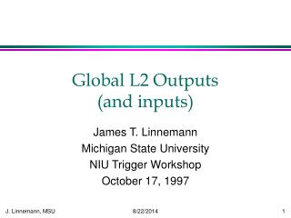

Inputs and Outputs
E N D
Presentation Transcript
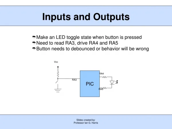
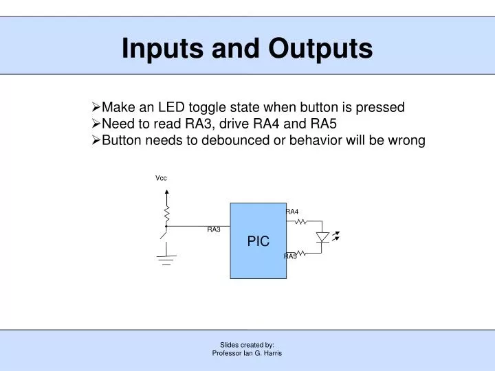
Slides created by: Professor Ian G. Harris Vcc PIC RA4 RA3 RA5 Inputs and Outputs • Make an LED toggle state when button is pressed • Need to read RA3, drive RA4 and RA5 • Button needs to debounced or behavior will be wrong
Slides created by: Professor Ian G. Harris Vcc PIC RA3 Debouncing Buttons • Mechanical bounce in switch causes signal to bounce • Noticable at MHz clock rates • Need to wait until signal settles before sampling it 10ms RA3
Slides created by: Professor Ian G. Harris i = 0; while (i < settletime) { if (RA3 == 0) i = 0; else i = i + 1; } • Reset counter • Advance counter Wait to Settle • settletime is the time a button signal must stay constant to be sure that it is settled • After a signal change, wait settletime clks • Debounce rising edge, reset counter every signal change to 0 • Need to debounce falling edge as well as rising edge
Slides created by: Professor Ian G. Harris Debouncing Toggle Code TRISA = 0b001111; PORTA = 0b111111; while (1 == 1) { i = 0; while (i < settletime) { if (RA3 == 0) i = 0; else i = i + 1; } i = 0; while (i < settletime) { if (RA3 == 1) i = 0; else i = i + 1; } RA5 = RA5 ^ 1; } • Make RA3 input, RA4, RA5 outputs • Wait for rising edge to settle • Wait for falling edge to settle • Toggle LED
Slides created by: Professor Ian G. Harris Analog to Digital Conversion • Built-in 10-bit analog-to-digital converter • Can read analog data from several different inputs • Controlled via 5 special registers ADRESH and ADRESL • Contain results of conversion • 10-bit result stored in 2 8-bit registers ADRESH ADRESL ADRESH ADRESL Right Justified Format Left Justified Format
Slides created by: Professor Ian G. Harris ADCON0 Register • Internal or external voltage reference can be used • ADC must be powered on before conversion
Slides created by: Professor Ian G. Harris ADCON1 Register • Conversion requires 11 conversion clocks • ADCON1<6:4> determine the frequency of the conversion clock • Minimum conversion time is 1.6 us Conv. Clk. ADCON1<6:4>
Slides created by: Professor Ian G. Harris RC3 RC2 RC1 RC0 RA3 RA2 RA1 RA0 ANSEL ANSEL Register • Some I/O pins can be configured as either digital or analog inputs • RA0:RA3, RC0:RC3 • ANSEL register bits correspond to these I/O • ANSEL ith bit = 1 means that input i is an analog input • TRIS bit for i must also be set to 1
Slides created by: Professor Ian G. Harris • Select analog inputs ANSEL = 0b00000001; // RA0 is an analog input • Set ADC parameters and power on ADCON0 = 0b 0 0 0 000 0 1; Power on ADC Left justified Vdd is reference Do not start Convert channel 0 (RA0) • Set conversion frequency ADCON1 = 0b0 011 0000; Internal clock, TAD = 4us Initializing ADC Conversion
Slides created by: Professor Ian G. Harris Performing ADC Conversion • Start conversion ADCON0 = ADCON0 | 0b00000010; GODONE = 1; • Wait for conversion to finish - ADC will clear GODONE bit when finished while (GODONE); • Get the result value result = ADRESH;
Slides created by: Professor Ian G. Harris Comparators • Comparator – compares two analog voltages • Outputs 1 if Vin+ > Vin- • The PIC contains two comparators • Very simple ADC Image taken from PIC16F684 Datasheet, Microchip Technology Inc.
Slides created by: Professor Ian G. Harris Comparator Inputs/Outputs • Comparators receive inputs from RA0, RA1 (C1) and RC0, RC1 (C2) • Comparator outputs appear in CMCON0 register, bits 6 and 7 • C1IN- is RA1 • C1IN+ is RA0 • C2IN- is RC1 • C2IN+ is RC0 Image taken from PIC16F684 Datasheet, Microchip Technology Inc. • C1OUT is (CMCON0 & 0b01000000) >> 6 • C2OUT is (CMCON0 & 0b10000000) >> 7
Slides created by: Professor Ian G. Harris Bit Name Function Invert output bits Comparator Control • CMCON0 register contains results and controls “mode” • Comparator mode determines comparator inputs and on/off • CIS selects comparator inputs in specific modes
Slides created by: Professor Ian G. Harris Comparator Modes Images taken from PIC16F684 Datasheet, Microchip Technology Inc. • Only mode 111 allows RA0, RA1, RC0, RC1 to be digital I/O CMCON0 = 0b00000111;