
SlideServe
Menu
Préférences
© SlideServe · v2026

Inputs and Outputs

tandice avatar
14 diapositives · 475 Views · Jun 08, 2012

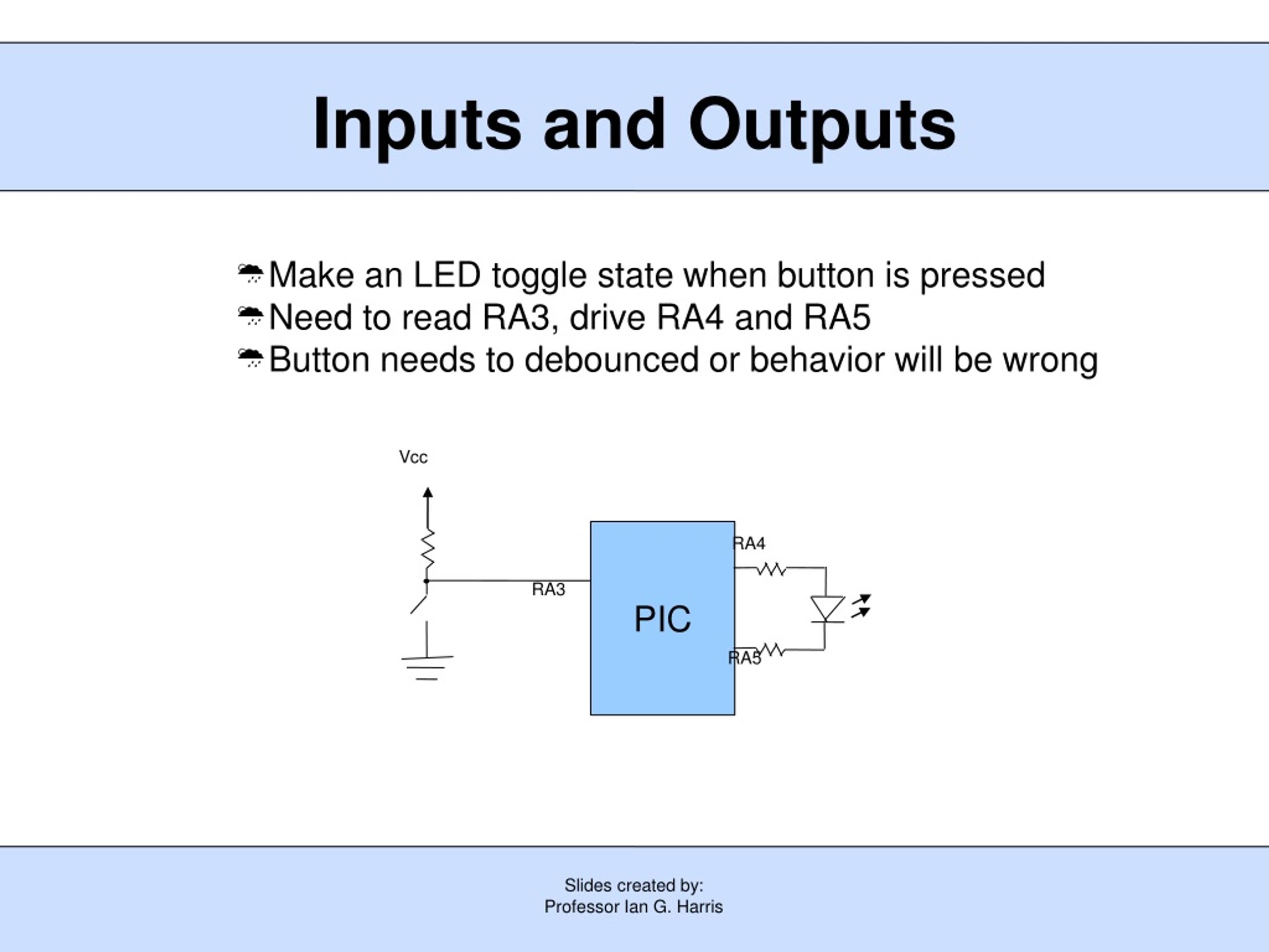
Vcc. PIC. RA4. RA3. RA5. Inputs and Outputs. Make an LED toggle state when button is pressed Need to read RA3, drive RA4 and RA5 Button needs to debounced or behavior will be wrong. Vcc. PIC. RA3. Debouncing Buttons. Mechanical bounce in switch causes signal to bounce
Inputs and Outputs - slide 1
01 / 14Inputs and Outputs
1 / 17

Télécharger la présentation

Inputs and Outputs
Une image / un lien ci-dessous est fourni (tel quel) pour télécharger la présentation

Politique de téléchargement : le contenu du site vous est fourni TEL QUEL pour votre information et votre usage personnel ; il ne peut être vendu, concédé sous licence ni partagé sur d’autres sites sans l’accord de son auteur.Le contenu vous est fourni TEL QUEL, pour votre information et votre usage personnel uniquement. Téléchargez la présentation en cliquant sur ce lien. Lors du téléchargement, si vous ne parvenez pas à télécharger une présentation, l’éditeur a peut-être supprimé le fichier de son serveur.Pendant le téléchargement, si vous ne parvenez pas à obtenir une présentation, le fichier a peut-être été supprimé par l’éditeur.

F I N

Plus de contenu associé

Transcription de la présentation
  1. Slides created by: Professor Ian G. Harris Vcc PIC RA4 RA3 RA5 Inputs and Outputs • Make an LED toggle state when button is pressed • Need to read RA3, drive RA4 and RA5 • Button needs to debounced or behavior will be wrong

  2. Slides created by: Professor Ian G. Harris Vcc PIC RA3 Debouncing Buttons • Mechanical bounce in switch causes signal to bounce • Noticable at MHz clock rates • Need to wait until signal settles before sampling it 10ms RA3

  3. Slides created by: Professor Ian G. Harris i = 0; while (i < settletime) { if (RA3 == 0) i = 0; else i = i + 1; } • Reset counter • Advance counter Wait to Settle • settletime is the time a button signal must stay constant to be sure that it is settled • After a signal change, wait settletime clks • Debounce rising edge, reset counter every signal change to 0 • Need to debounce falling edge as well as rising edge

  4. Slides created by: Professor Ian G. Harris Debouncing Toggle Code TRISA = 0b001111; PORTA = 0b111111; while (1 == 1) { i = 0; while (i < settletime) { if (RA3 == 0) i = 0; else i = i + 1; } i = 0; while (i < settletime) { if (RA3 == 1) i = 0; else i = i + 1; } RA5 = RA5 ^ 1; } • Make RA3 input, RA4, RA5 outputs • Wait for rising edge to settle • Wait for falling edge to settle • Toggle LED

  5. Slides created by: Professor Ian G. Harris Analog to Digital Conversion • Built-in 10-bit analog-to-digital converter • Can read analog data from several different inputs • Controlled via 5 special registers ADRESH and ADRESL • Contain results of conversion • 10-bit result stored in 2 8-bit registers ADRESH ADRESL ADRESH ADRESL Right Justified Format Left Justified Format

  6. Slides created by: Professor Ian G. Harris ADCON0 Register • Internal or external voltage reference can be used • ADC must be powered on before conversion

  7. Slides created by: Professor Ian G. Harris ADCON1 Register • Conversion requires 11 conversion clocks • ADCON1<6:4> determine the frequency of the conversion clock • Minimum conversion time is 1.6 us Conv. Clk. ADCON1<6:4>

  8. Slides created by: Professor Ian G. Harris RC3 RC2 RC1 RC0 RA3 RA2 RA1 RA0 ANSEL ANSEL Register • Some I/O pins can be configured as either digital or analog inputs • RA0:RA3, RC0:RC3 • ANSEL register bits correspond to these I/O • ANSEL ith bit = 1 means that input i is an analog input • TRIS bit for i must also be set to 1

  9. Slides created by: Professor Ian G. Harris • Select analog inputs ANSEL = 0b00000001; // RA0 is an analog input • Set ADC parameters and power on ADCON0 = 0b 0 0 0 000 0 1; Power on ADC Left justified Vdd is reference Do not start Convert channel 0 (RA0) • Set conversion frequency ADCON1 = 0b0 011 0000; Internal clock, TAD = 4us Initializing ADC Conversion

  10. Slides created by: Professor Ian G. Harris Performing ADC Conversion • Start conversion ADCON0 = ADCON0 | 0b00000010; GODONE = 1; • Wait for conversion to finish - ADC will clear GODONE bit when finished while (GODONE); • Get the result value result = ADRESH;

  11. Slides created by: Professor Ian G. Harris Comparators • Comparator – compares two analog voltages • Outputs 1 if Vin+ > Vin- • The PIC contains two comparators • Very simple ADC Image taken from PIC16F684 Datasheet, Microchip Technology Inc.

  12. Slides created by: Professor Ian G. Harris Comparator Inputs/Outputs • Comparators receive inputs from RA0, RA1 (C1) and RC0, RC1 (C2) • Comparator outputs appear in CMCON0 register, bits 6 and 7 • C1IN- is RA1 • C1IN+ is RA0 • C2IN- is RC1 • C2IN+ is RC0 Image taken from PIC16F684 Datasheet, Microchip Technology Inc. • C1OUT is (CMCON0 & 0b01000000) >> 6 • C2OUT is (CMCON0 & 0b10000000) >> 7

  13. Slides created by: Professor Ian G. Harris Bit Name Function Invert output bits Comparator Control • CMCON0 register contains results and controls “mode” • Comparator mode determines comparator inputs and on/off • CIS selects comparator inputs in specific modes

  14. Slides created by: Professor Ian G. Harris Comparator Modes Images taken from PIC16F684 Datasheet, Microchip Technology Inc. • Only mode 111 allows RA0, RA1, RC0, RC1 to be digital I/O CMCON0 = 0b00000111;