Download
1 / 24
240 likes | 352 Vues
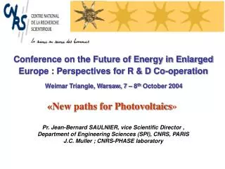
Conference on the Future of Energy in Enlarged Europe : Perspectives for R & D Co-operation. Weimar Triangle, Warsaw, 7 – 8 th October 2004. «New paths for Photovoltaics » Pr. Jean-Bernard SAULNIER, vice Scientific Director , Department of Engineering Sciences (SPI), CNRS, PARIS

E N D
Conference on the Future of Energy in Enlarged Europe : Perspectives for R & D Co-operation Weimar Triangle, Warsaw, 7 – 8th October 2004 «New paths for Photovoltaics» Pr. Jean-Bernard SAULNIER, vice Scientific Director , Department of Engineering Sciences (SPI), CNRS, PARIS J.C. Muller ; CNRS-PHASE laboratory
Summary PV : a need for research ? The main keys: Efficiency, cost Hierarchic perspectives : Short, mean and long term An overview of CNRS research forces
Great variety of applications From space to terrestrial use Off grid Telecom Lightning Pumps, refrigerators Building Consumers products Grid connected (distributed, centralized) Source : PV Energy Syst.Fev. 2002
World production of modules ~ 500 MW (2002), ~34% /year => 1 GW ~ 2005 Driven PV roofs: Japan 70 000 Germany 100 000 France 10 000 Source : PV News, feb/ may 2003
Non uniform market (MW) Off grid: France Grid connected : Germany, Japan nuclear Si 4-6 €/ W installed 30-50 c€ / kWh 3 c€ /kWh
Technologies Bulk Crystalline Silicon : 85% Thin films : 15% Amorphous Si… Chalcogenides Organic Quantum cells Systems
Evolution of technologies : efficiencies A. Goetzberger & J. Luther, FhG-ISE (DE) 1st : Bulk Si : sc/mc-Si (85%) 2nd : thin film : Si ribbon (3%) a-Si (4 %), CIS (1 %), c-Si & organic 3rd : new. materials
Which issues for these technologies? • Bulk-Si Modules & Systems • 4-6 € /Wc and 30-50 c€ / kWh Reduce : Cost/ Efficiency • Reduce impact of raw material • Improve the management of integrated systems in grids & and in buildings Thin filmsIndustrial Development Faster processes & larger surfaces Efficiencies 12 à 15 % (modules) Materials & concepts for future Improve stability (ex :organic 3% < 500 h)
Short Term Prospective: < 5 years • Crystalline bulk Silicon • Decrease impact of raw material: • Purification of metallurgical Si : plasma processes • Thinner wafers or ribbons(30-150 µm) • New electro-chemical sawing processes:less losses • Projects: ADEME-PW-CEA-CNRS Reducop et Sinergies • Grid Integration ofmulti-sourcesSystems • Smart converters, storage, securized
UNSW CNRS Photowatt Source : GIT (USA) 2000 Multi-cristallineSilicon : mc-Si Projects: Reducop & Sinergies(ADEME-PW-CEA-CNRS :2004-2007) Objectives:18% - 20% et 0,8-1,0€ / W Progresses: program PV16 ADEME/CNRS PHOTOWATT 1999-2003 16%, 2 €/W
Mean Term Prospective : mean term 5 to 15 years • Industrial Development of thin films • Fast processes, higher efficiency and larger surfaces • Si crystalline • large grains / transfer of crystalline-Si • Amorphous/pm/µc-Si • transfer pm-Si to industry (FEE, SOLEMS, UNAXIS) • new tandem Si/SiGe and Si/µcSi cells • hetero-structures (HIT) • Chalcogenides (CIS) • 2 ways: electro-chemical (CISEL project) and dry processes • towards modules (30X30cm)
Photons Contact - ZnO CdS Contact + CuInSe2 Molybdène Verre Source : P. Roca, LPICM Ecole Polytechnique Alternativethin films: CIS Heterojunctions with polycrystalline thin films «Crystalline Si performances for the price of amorphous » • Co-evaporation: Dry technology, exploration of new compounds • Electro-deposition:CISEL Project (CNRS-EDF-St Gobain) Source : J.F. Guillemoles, LECA
Long Term Prospective: (> 15 years) Potentialities of new materials and of new concepts OrganicMaterials : New Project (2002) increase stability (500 h) Identification of materials : co-polymers, new molecules, fullerensdérivative, pigments Active layers: imbricated networks, liquid crystals The point with interfaces in the cells
OrganicComposites Polymers : present situation: h = 3.5 % (Un. Linz Austria) Dérivate from fulleren C60 France JM NUNZI: 2.9 %
Long term Prospective : (> 15 yearss) New materials and concepts (foll.) New tandem structures : luminescence & multi-photons conversion compositematerials : modified host matrix by adding nano-cristallites (Si,Ge), nano-particules matrix and species: mineral or organic ======= Power Components power conversion integration within the cell
M convertisseur SC 3rd Génération Cells Concepts to explore : • Structure « hot carriers » : • luminescence • multi-photons UV nano-particules: minéral (Si, Ge, …) or organic • Structure « strong absorption » IR quantum dots, …
PHOTOVOLTAICS Priorities Priority I: Basic Research on nano-structured materials for inter-conversion of photons : mineral/organicnanocristallites CEA PI « Full-spectrum » FP 6: accepted Priority II: Mastering interfaces in hetero-structures in thin films(Si, CIS, organic) ==> high efficiency + low cost CIS team PI FP 6: complementary list Priority III: Ultimate Technologies for thin cristalline silicon wafers ==> low cost PHOTOWATT & CNRS-PHASE PI « Crystal-clear » FP 6 : accepted
PHOTOVOLTAIQUE Platforms • « RESTORE » national project 4-5 ans « Sinergies » (> 5x5 cm2): • ADEME-CEA-CNRS (PHOTOWATT) • => transfer of process to industry • Platform CIS : « CISEL »project(CNRS-EDF-St GOBAIN) • From the lab module => to industrial concept • Research Platform : • composite and nanostructured materials « Process PV » • =>laboratorydemonstrators < cm2 (Strasbourg) A new Solar Institute CNRS / CEA in Chambéry : INES
Implantation Map CNRS : 80 seniors 1ère génération Région Grenobloise: «Sinergies » 2ème génération Région Parisienne: « CISEL » 3ème génération Région Alsace: « Process PV »
Conference on the Future of Energy in Enlarged Europe : Perspectives for R & D Co-operation Weimar Triangle, Warsaw, 7 – 8th October 2004 «New paths for Photovoltaics» Pr. Jean-Bernard SAULNIER, vice Scientific Director , Department of Engineering Sciences (SPI), CNRS, PARIS J.C. Muller ; CNRS-PHASE laboratory
World production of modules ~ 500 MW (2002), ~34% /year => 1 GW ~ 2005 Driven PV roofs: Japan 70 000 Germany 100 000 France 10 000 Source : PV Energy Syst.Fev. 2002
Production verticalement intégrée Lingot cristallisé 240 Kg Découpe des briques Découpe des wafers (sciage à fil) Fabrication des cellules Assemblage des modules
Matériaux Semi-conducteurs pour le photovoltaïque Cellule tandem à base de CuGaSe2/CuInSe2
Emetteur n+ Contact p p-Si p+ Si substrat Si cristallin en couches minces Source : A. Slaoui, CNRS-PHASE • Substrats céramiques :mullite, SiSiC, SiN • Grands grains-cristallisation induite par métaux • - dépôts sur surface liquide • - transfert de sc-Si