Download
1 / 41
430 likes | 632 Vues
In The Name Of God. Design And Implementation Of Frequency Synthesizer And Interrogating Phase Noise In It's Parts. Advisor Professor : Dr.Sadr & Dr.Tayarani Students: Majid Sodagar Mehran Mohammadi Izad. Brief Review. Introduction Block Diagrams Models Oscillator Divider

E N D
In The Name Of God Design And Implementation Of Frequency Synthesizer And Interrogating Phase NoiseIn It's Parts Advisor Professor : Dr.Sadr & Dr.Tayarani Students: Majid Sodagar Mehran Mohammadi Izad
Brief Review • Introduction • Block Diagrams • Models • Oscillator • Divider • Charge Pump • Design And Measurements • Conclusions
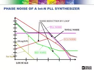
Introduction & Motivation • The GSM system needs very narrow channel spacing • Thus low phase noise levels are required. • e.g. , At 1 kHz from the carrier, a single sided spectral noise density of -80 dBc/Hz
Oscillator Noise Modeling • LTI Model (Leeson-Cutler) - Ignoring Time Variance Nature of Oscillator • LTV Model (Hajimiri-Lee) - Take the Time Variance Nature of Oscillator into account.
Typical LC Oscillator A = Excess noise FactorN = For Active Inductor
LTI Model Using Only Z(s) of tank circuit
LTV Model • Every oscillator is a quasi periodic system • the noise analysis should take this into account • Model Benefits: • Design Aspects • Cyclostationary noise
Impulse Response The constant qmax = CVpeak is simply a normalization constant, the peak charge in the oscillator.
Filter Noise • Ignoring Thermal noise of Passive elements And Current Noise
Typical OpAmp Input Voltage Noise • Our OpAmp Performance (OP27):
Charge Pump PFD Structure • Lead And Lag Detection • Increasing Lock Range • Reduction of cycle slipping
Effects Of CP PFD On Phase Noise • Effect of Leakage On reference Spurs • Charge pump is off majority of the Time • Leakage causes VCO tuning voltage to change • Effect of Mismatch On reference Spurs • The width of correction pulses is related to the mismatch • causes the AC voltages • undesirable AC voltages Causes FM modulation
Experimental Results for FM modulation (Spurs) Reference Spur example
CP Phase noise model • Where • Fc = Flicker Corner Frequency • Fm = Offset From Carrier • I0 = current noise Floor
The charge pump nature is discrete so it is prone to instability The following condition should be satisfied to use continuous time analysis !! Stability problem In CP PLL
Design Specification • Design for GSM requirements • Fref = 10MHz • Fcomp = 200KHz • LoopBandWidth = 15KHz • RFOut = 800 – 1100 MHz • PhaseMargin = 45 deg
Passive Phase Noise Result @1KHz Phase noise = -53.7-10log(200) = -76.7 dBc/Hz
Passive Phase Noise Result @10KHz Phase noise = -51.9-10log(200) = -74.9 dBc/Hz
Passive Phase Noise Result @100KHz Phase noise = -70.2-10log(500) = -92.9 dBc/Hz
Step Response And Lock Time • Settling time = 150msec
Active Phase Noise Result @1KHz Phase noise =-55.1-10log(200)= -78.1 dBc/Hz
Active Phase Noise Result @10KHz Phase noise =-49.7-10log(200)=-72.7 dBc/Hz
Inappropriate Opamp Bias !!! Causing excess noise near the career
1Hz Normalize Phase Noise • Good way for characterize the phase noise of PLL • Assumes charge pump phase noise is dominant • PN=PN1Hz+20logN+10log(Fcomp)
Experimental Result: • For our design: • PN1Hz = -205 dBc/Hz • N = 4500 • Fcomp = 200KHz • PN =-205+20log(4500) +10log(200KHz) = -78.9 dBc/Hz
Conclusions • By using better synthesizer, its possible to achieve lower Phase noise • If the CP noise Dominates in the circuit, then we can not detect the effect of Active filter noise