Lecture 13 High-Gain Differential Amplifier Design
280 likes | 724 Vues
Lecture 13 High-Gain Differential Amplifier Design. Woodward Yang School of Engineering and Applied Sciences Harvard University woody@eecs.harvard.edu. Overview. Background

Lecture 13 High-Gain Differential Amplifier Design
E N D
Presentation Transcript
Lecture 13High-Gain Differential Amplifier Design Woodward Yang School of Engineering and Applied Sciences Harvard University woody@eecs.harvard.edu
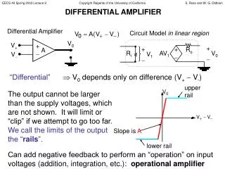
Overview • Background This lecture investigates different topologies (and their characteristics) that can be used to implement differential amplifiers with extremely high gain. We will again be using cascoding. ES154 - Lecture 13
Review of Amplifier Characteristics • Let’s review some of the characteristics of the different (single-ended) amplifier topologies that we’ve looked at so far. • We will augment this table when we look at the frequency response characteristics of these amplifiers ES154 - Lecture 13
Multi-Stage Amplifiers (Cascading) • We can cascade different types of amplifiers to get desired overall characteristics. Often want: • High input impedance • High gain • Low output impedance • Mix and match cascades of different types of amplifiers to get desired result ES154 - Lecture 13
Common-Emitter Emitter-Follower Cascade • A common configuration (for discrete BJT amplifier design) is a common-emitter emitter-follower (common-collector) cascade • CE stage has high voltage gain and high input impedance • CC stage has low output impedance to drive various load conditions • CC stage also presents a high impedance load to the CE amplifier which enables high voltage gain for the CE stage ES154 - Lecture 13
Common-Source Source-Follower Cascade • Similarly, cascade a common-source amplifier with a source-follower. ES154 - Lecture 13
Building Op Amps • Op amps are an important component of modern CMOS IC’s. They used to designed as general purpose amplifiers that can meet a variety of requirements. The main target was extremely high gain (>1e5), high input impedance and low output impedance (like an ideal amplifier). This was done (to some extent) at the expense of different aspects of performance (e.g., speed, output voltage range, power, etc.). Designs these days are much more tailored to have (good enough) performance w.r.t. the specific needs of particular applications. Within an IC, often use Operational Transconductance Amplifiers (OTA). • Some performance parameters of op amps • Gain and Bandwidth • Want as large as possible • Output Swing • Maximize w.r.t. power supply (but supply shrinking in modern processes) • Linearity • Combat non-linearity with feedback • Noise and Offset • Can minimize by trading off other parameters • Supply Rejection • Strong dependence on current source output resistance ES154 - Lecture 13
Simple One-Stage Op Amps • Two differential pair amplifiers that we have already seen can be used as op amps. The low-frequency, small-signal gain of both is gmN(roN||roP). The capacitive loads (CL) usually determine their bandwidth. ES154 - Lecture 13
Cascoded Amplifier • Use cascoding to increase load resistance • Cascode both the active loads and the differential pair • Higher effective load resistance • Higher ro for the differential pair • Reduces Miller effect (will see later) • However, there are some limitations • Reduced output swing (must keep all devices in saturation) • What is the output dynamic range? • How might one increase the output swing range for vo? ES154 - Lecture 13
Use High-Swing Cascodes • We can use the high-swing cascode circuit as a load to achieve higher output range in a single-ended output telescopic amp ES154 - Lecture 13
Cascode Op Amps • Amplifiers that use cascoding are often called ‘telescopic’ cascode amps. While gain increases, the output range of these devices are limited. • Connecting in unity-gain feedback configuration results in significant reduction of output range ES154 - Lecture 13
DC Biasing for High-Gain Amplifiers • One of the challenges of using cascodes for high gain is appropriately setting the DC biasing for the circuit. Let’s look at an example… • What is the raitio of ILOAD vs. ITAIL? ES154 - Lecture 13
DC Biasing Cont’d • Strategy for setting up DC bias • All transistors should be saturation • Set VBNC so that differential input pair in saturation • Want to set it to the edge with sufficient saturation margin (~300mV) • Set VBP so that ILOAD = ITAIL/2 • Set VBPC so that pMOS currnet source loads are close to edge of saturation • Need to set VBP and VBPC carefully to keep devices in saturation and the DC common mode of the output nodes to be in the middle of the output swing range • This can be challenging to do due to the high output resistance at the output. • Would be nice if there was a way to automatically set the biasing… ES154 - Lecture 13
Common-Mode Feedback Biasing • Use an amplifier to set the pMOS current source with respect to some desired output common-mode voltage (VREF). ES154 - Lecture 13
CM FB Biasing • Here’s how it works: • Use large resistors to find the average (common-mode) output voltage • An amplifier compares VREF to VOUT,CM and sets VBP such that VOUT,CM = VREF • Let’s understand how it works • What happens to VBP if VREF increases? • What happens to VBP if VOUT,CM increases? ES154 - Lecture 13
Folded Cascode Circuit • In order to alleviate some of the drawbacks of telescopic op amps (limited output range), a “folded cascode” can be used • M1 is common-source transconductance amp and M2 is common-gate transimpedance amp • Advantage is M2 no longer stacks on top of M1 • Possible for either pMOS or nMOS cascodes • The output resistance for cascode and folded cascode are roughly equivalent (gmro2) ES154 - Lecture 13
Folded Cascode Amplifier • Turn a differential telescopic cascode amplifier into a folded cascode amplifier ES154 - Lecture 13
Full circuit Implementation of Folded Cascode Amplifier • Reference current sources are set: • A version with nMOS differential pair inputs also possible (flip upside down) • What sets output common mode? • Depends on relative output resistances looking up and down • Can vary with process and reference current mismatches ES154 - Lecture 13
Gain of a Folded-Cascode Amplifier • Calculate gain using the differential half-circuit. Gain can be calculated as GmRout where Gm is the short-circuit transconductance of the overall circuit and Rout is the output resistance. • Short out Vout to ground and solve for Iout/Vin = Gm • Solve for the output resistance ES154 - Lecture 13
Common-Mode Feedback • Use feedback to set the output common mode of a folded cascode amplifier, called common-mode feedback • Sense the average (common-mode) voltage at the output, compare to a desired reference voltage (Vref), and use it to set the current source • For Vin=0, feedback sets IFB=IREF2+IREF1/2 and common-mode voltage = Vref ES154 - Lecture 13
Two-Stage Op Amps • In order to implement amplifiers with high gain and high swing, we must resort to two-stage amplifier designs • First stage used to generate high gain • Second stage to generate high swing • Use any high-gain first stage and high-swing second stage • two simple examples (differential and single-ended output amplifiers) ES154 - Lecture 13