Download
1 / 16
Combinational Circuit Design: Study Guide with Gate Delays and Hazards
180 likes | 300 Vues
This chapter covers combinatorial circuit design, gate fan-in limits, gate delays, timing diagrams, hazards in logic, simulation, and testing. Includes design problems and figures. Learn to analyze and optimize logic circuits.
Télécharger la présentation 
Combinational Circuit Design: Study Guide with Gate Delays and Hazards
An Image/Link below is provided (as is) to download presentation
Download Policy: Content on the Website is provided to you AS IS for your information and personal use and may not be sold / licensed / shared on other websites without getting consent from its author.
Content is provided to you AS IS for your information and personal use only.
Download presentation by click this link.
While downloading, if for some reason you are not able to download a presentation, the publisher may have deleted the file from their server.
During download, if you can't get a presentation, the file might be deleted by the publisher.
E N D
Presentation Transcript
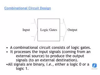
This chapter in the book includes: Objectives Study Guide 8.1 Review of Combinational Circuit Design 8.2 Design Circuits with Limited Gate Fan-In 8.3 Gate Delays and Timing Diagrams 8.4 Hazards in Combinational Logic 8.5 Simulation and Testing of Logic Circuits Problems Design Problems FIGURES FORCHAPTER 8COMBINATIONAL CIRCUIT DESIGN AND SIMULATION USING GATES Click the mouse to move to the next page. Use the ESC key to exit this chapter.


More Related