Download
1 / 21
210 likes | 322 Vues
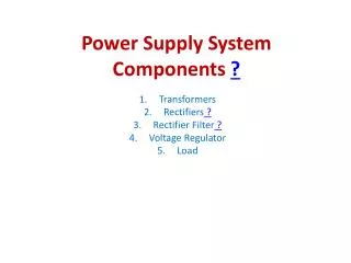
The power supply system of the AMS experiment tracker detector, divided into subunits with DC-DC converters, filters, and boards, underwent rigorous qualification tests for reliability. Components were tested for Total Dose and SEE, thermovacuum, thermo-mechanical, and EMI/EMC compatibility. Conclusions showed functionality and compliance with safety standards.

E N D
The power supply system of the AMS experiment M. Menichelli, L. Accardo, G. Ambrosi, R. Battiston, M. Bizzarri, S. Blasko, D. Cosson, E. M. Fiori, O. Maris, A. Papi, G. Scolieri. INFN Sezione di Perugia
The System • The power supply system of the AMS tracker detector is divided into 8 subunits each subunit takes power from one 28 VDC output of the PDS (Power Distribution system) common for the entire apparatus. • Each subunit is composed by: • a TPD (Tracker Power Distributor) that contains DC-DC converters, input filter and an interface board with the slow control system. • A crate which hosts linear regulator board, (for bias generation and for powering the front-end electronics) readout cards (TDR tracker data reduction) and the interface with the main slow control and data collection system (called JINF)
The TPD I • a dual input filter (S9011B) • an interface board that controls and monitor the status of various DC-DC converters.(S9011A) • 4 dual S9051 (all active) DC-DC converters having output ±2.5 V and 5.6 V for powering the front-end circuits. • 2 dual S9053 (1 active, 1 spare each board) DC-DC converters having 3.4 V output for poweing the digital electronics • 2 dual S9055 (1 active, 1 spare each board) DC-DC converters having 120 V and ±6 V for biasing the detector and powering the linear regulators inside the TBS
The crate • 12 TDR boards for ladder readout. • 1 JINF board for data comunication and slow control interface for the entire crate. • 4 TPSFE linear regulator boards for the front-end circuits • 2 TBS linear regulator for the bias.
The qualification tests • The radiation tests • The thermovacuum test • The thermo mechanical test • The EMI/EMC test
The thermo mechanical test I • Phase 1: 10 thermal cycles between +85 °C and –45 ° on air not powered • Phase 2: 4 minute each axe random vibration test (3 axes) • Phase 3: 5 thermal cycles between +85 °C and –45 ° on air not powered
The EMC/EMI I • Derived from MIL-STD-461 • CE101 (30Hz - 10 kHz) • CE102 (10 kHz- 50 MHz) • CS101 (30 Hz-150 kHz) • RE101 (30 Hz-100 kHz) • RE102 (10 kHz-2 GHz) • RS101 (30 Hz-100 kHz) • RS102 (10 kHz-1 GHz)
Conclusions • The cards were functional after the various tests. • The thermal probes placed on the various cards did not show presence of any hot spot. • During the vibration test the resonances found on the cards where well above the safety limit of 50 Hz • The measured levels of emitted and conducted noise on the EMC/EMI tests where below the limits • The cards remained functional under the perturbation during the susceptibility tests • All The QM cards tested where validated for further production