
SlideServe
Menu
Préférences
© SlideServe · v2026

Advanced PCB Inspection Systems Optimizing Production Processes

saber avatar
17 diapositives · 315 Views · Aug 29, 2014

Explore cutting-edge inspection technologies in PCB manufacturing, focusing on advanced inspection systems that enhance efficiency and accuracy. Discover the benefits of automated optical inspection (AOI), stencil cleaning, precise alignment, and post-print evaluations. Our systems offer detailed detection capabilities for paste on pads, bridging, print offsets, and stencil issues. Comparative analyses show the speed of inspections across different machines, with an emphasis on reducing operator errors and setup time. Achieve 100% inspection rates and guarantee high-resolution imaging for reliable production processes.
Advanced PCB Inspection Systems Optimizing Production Processes - slide 1
01 / 17Advanced PCB Inspection Systems Optimizing Production Processes
1 / 17

Télécharger la présentation

Advanced PCB Inspection Systems Optimizing Production Processes
Une image / un lien ci-dessous est fourni (tel quel) pour télécharger la présentation

Politique de téléchargement : le contenu du site vous est fourni TEL QUEL pour votre information et votre usage personnel ; il ne peut être vendu, concédé sous licence ni partagé sur d’autres sites sans l’accord de son auteur.Le contenu vous est fourni TEL QUEL, pour votre information et votre usage personnel uniquement. Téléchargez la présentation en cliquant sur ce lien. Lors du téléchargement, si vous ne parvenez pas à télécharger une présentation, l’éditeur a peut-être supprimé le fichier de son serveur.Pendant le téléchargement, si vous ne parvenez pas à obtenir une présentation, le fichier a peut-être été supprimé par l’éditeur.

F I N

Plus de contenu associé

Transcription de la présentation
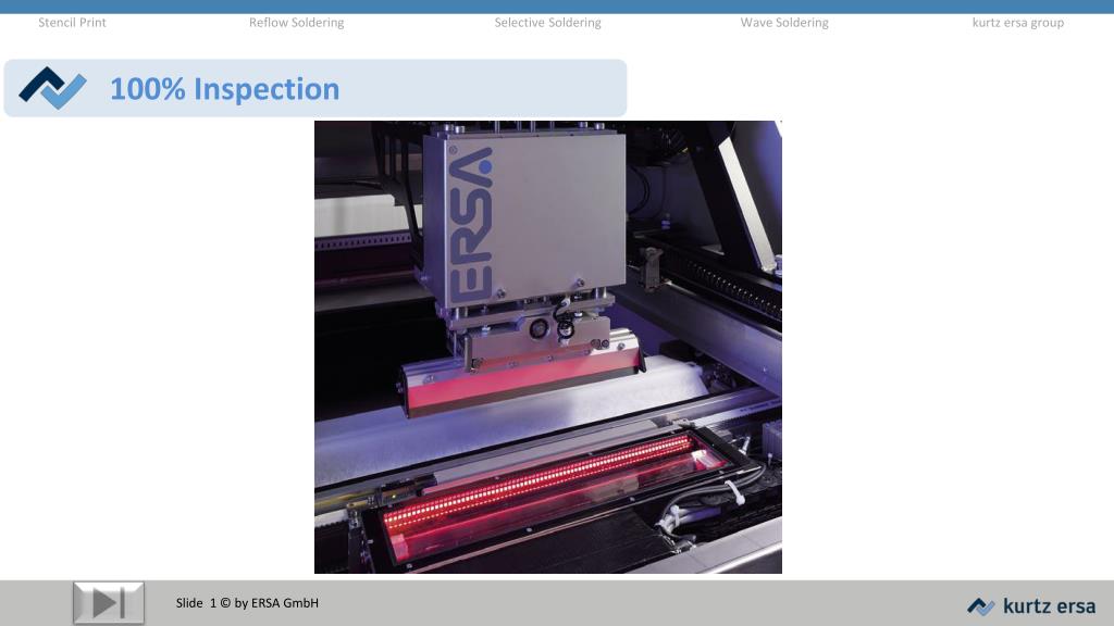
  1. 100% Inspection

  2. print inspection transport ProcessSteps stencilcleaning alignment

  3. AOI AOI AOI Post-Print 1% 20% Post-Placement Post-Reflow 19% 60% Quelle: CyberOptics ProcessSteps Print Place Reflow Mistakes Other Postionof AOI

  4. X & AOI ProcessSteps Print Place Reflow Lowinvest- lessfloorspace– onecontact!

  5. VERSAPRINT Inspection Systems Detectionofpaste on Pad Detectionofbridges Detectionofprintoffset Detectionofstencilsmearingandblockage AOI Inside

  6. DetectionofPrinf Offset

  7. Detectionof Paste on Pad

  8. L I S T LIST (Line Scan Technology)

  9. Reflector Cube Stencil Light Source 2 (spot) Light Source 1 (spot) CCD Cam. CCD Cam. Lens Diffused Lightsource Substrate Source: EKRA Illumination Cube Stencil Light Source 1 CCD Camera Prism Light Source 2 Substrate Source: EKRA ConventionalCamera Systems I. II.

  10. New Line Scan Technology Camera System Stencil PCB One Axis, Two Pictures, Three Goals: Precise, Fast, Easy!

  11. Diffuse Direct HAND SOLDERING Diffuse andDirect Light Source LED Direct light source Diffuse light source Two different light sourcesguarantee a reliabledetectionof: Paste on pad andbridging Rod Lens Image Sensor

  12. LIST Camera High Speed, Full Area Scan Stencil PCB 260 mm @ 35 mm/sec.!

  13. LIST Process Advantage: Teach in • Scanning thewholesubstrateenablestheoperatortosetupandteachtheprintervery easy • Minimisingofoperatorerrors

  14. ComparisonofInspection Speeds Manufacturer information

  15. Inspectionarea: 10,2% Inspectionarea: 100% Inspectionarea: 2% Inspectionarea: 2,7% Compareofinspectionspeedandarea ERSA P1 machineC machineB machineA P 7s I 3s P 7s I 1s P 7s I 2,5s P 7s I 8s C 1,5s C 3s C 3s C 3s T 4s T 6s T 6s T 6s Cycle time: 17s Cycle time: 17s Cycle time: 17s Cycle time: 17s 220mm x 160mm 220mm x 160mm 220mm x 160mm 220mm x 160mm

  16. I 29,3s I 36,9s I 129,3s I 8s cycle time: 43,3s cycle time: 52,9s cycle time: 143,8s cycle time: 17s Compareofinspectionspeedat 100% inspectionarea ERSA P1 machine B machine C machine A P 7s P 7s P 7s P 7s C 1,5s C 3s T 4s C 3s T 6s T 6s C 3s T 6s 220mm x 160mm 220mm x 160mm 220mm x 160mm 220mm x 160mm Inspectionarea: 100% Inspektion area: 100% Inspektion area: 100% Inspektion area: 100%

  17. LIST Process Advantages 100 %inspektion in linespeed Fullareainspectionof PCB layout High resolutionanddistortionfreepicture