Frequency Response & Resonant Circuits
Frequency Response & Resonant Circuits. Filters, frequency response, time domain connection, bode plots, resonant circuits. Outline and topics. Reading Boylestad Ch 21.1-21.11 Boylestad Ch 20.1-20.8. Low-pass filters High-pass filters Other filters Resonance (Ch 20)

Frequency Response & Resonant Circuits
E N D
Presentation Transcript
Frequency Response & Resonant Circuits Filters, frequency response, time domain connection, bode plots, resonant circuits.
Outline and topics Reading Boylestad Ch 21.1-21.11 Boylestad Ch 20.1-20.8 • Low-pass filters • High-pass filters • Other filters • Resonance (Ch 20) • Ideal op-amps and active filters • Decibels & log scales • Linear systems and transfer functions • Bode plots
FILTERS • Any combination of passive (R, L, and C) and/or active (transistors or operational amplifiers) elements designed to select or reject a band of frequencies is called a filter. • In communication systems, filters are used to pass those frequencies containing the desired information and to reject the remaining frequencies.
FILTERS • In general, there are two classifications of filters: • Passive filters-gain always<1 • Active filters-gain can be >1 Gain=Vo/Vi Can also be represented By a differential eqn. Circuit or system T(jω)=T(s) Vo Vi Gain works for DC always For AC, only for amplitude/phase of sine/cosine
FILTERS Couple of definitions: Impedance of a circuit element is the AC analog of resistance. Only works for sines and cosines! Z-impedance R-real part of impedance-resistance X-imag part of impedance-REACTANCE Resistance is always positive Reactance can be positive or negative Positive reactance-inductive Negative reactance-capacitive FIG. 21.7 Defining the four broad categories of filters.
FILTERS Impedance of a circuit element is the AC analog of resistance. Only works for sines and cosines! WHY? if input and output are sine or cosine, we can represent them as Why? Then, the “resistance-like” ratio of the amplitudes of current and voltage FIG. 21.7 Defining the four broad categories of filters.
FIG. 21.9 R-C low-pass filter at low frequencies. FIG. 21.8 Low-pass filter. R-C LOW-PASS FILTER
FIG. 21.10 R-C low-pass filter at high frequencies. FIG. 21.11 Vo versus frequency for a low-pass R-C filter. R-C LOW-PASS FILTER We must take the magnitude To get the size of the gain. This magnitude gives rise to the square root we see in the textbook. We take the “argument” or angle To get the phase of the gain. Applying voltage divider Zc-impedance Xc-reactance
FIG. 21.12 Normalized plot of Fig. 21.11. R-C LOW-PASS FILTER Links to help with sketching sines and cosines http://www.youtube.com/watch?v=ijTIr-aykUk&feature=relmfu http://www.youtube.com/watch?feature=endscreen&v=RzZyyIu9IvA&NR=1 At a given frequency, gain is a complex number that can be drawn as Imaginary/”reactive” Length is amplitude gain θ-phase change Real
FIG. 21.13 Angle by which Vo leads Vi. R-C LOW-PASS FILTER-PHASE
FIG. 21.14 Angle by which Vo lags Vi. R-C LOW-PASS FILTER
FIG. 21.15 Low-pass R-L filter. FIG. 21.16 Example 21.5. R-C LOW-PASS FILTER
FIG. 21.17 Frequency response for the low-pass R-C network in Fig. 21.16. R-C LOW-PASS FILTER Remember,
FIG. 21.18 Normalized plot of Fig. 21.17. R-C LOW-PASS FILTER
FIG. 21.19 High-pass filter. R-C HIGH-PASS FILTER
FIG. 21.20 R-C high-pass filter at very high frequencies. FIG. 21.21 R-C high-pass filter at f =0 Hz. R-C HIGH-PASS FILTER As w=0, |gain|=0 As winf, |gain|1
FIG. 21.22 Vo versus frequency for a high-pass R-C filter. R-C HIGH-PASS FILTER
FIG. 21.23 Normalized plot of Fig. 21.22. R-C HIGH-PASS FILTER
FIG. 21.24 Phase-angle response for the high-pass R-C filter. R-C HIGH-PASS FILTER Same as Boylestad result
FIG. 21.25 High-pass R-L filter. R-L HIGH-PASS FILTER What is L/R? w=0, |gain|=0 winf., |gain|1 What kind of filter is this?
FIG. 21.26 Normalized plots for a low-pass and a high-pass filter using the same elements. R-L HIGH-PASS FILTER
FIG. 21.27 Phase plots for a low-pass and a high-pass filter using the same elements. R-L HIGH-PASS FILTER
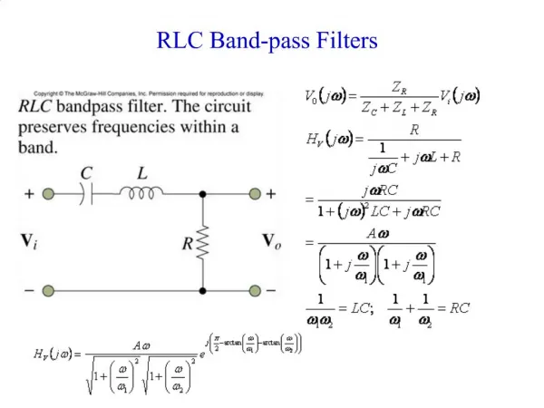
FIG. 21.28 Series resonant pass-band filter. PASS-BAND FILTERS CR gives you high pass, LR gives you low pass.
RLC Circuits-resonance! • The resonant electrical circuit must have both inductance and capacitance. • In addition, resistance will always be present due either to the lack of ideal elements or to the control offered on the shape of the resonance curve. • When resonance occurs due to the application of the proper frequency ( fr), the energy absorbed by one reactive element is the same as that released by another reactive element within the system.
SERIES RESONANT CIRCUIT • A resonant circuit (series or parallel) must have an inductive and a capacitive element. • A resistive element is always present due to the internal resistance of the source (Rs), the internal resistance of the inductor (Rl), and any added resistance to control the shape of the response curve (Rdesign).
FIG. 21.28 Series resonant pass-band filter. SERIES RESONANT CIRCUIT reactance At resonance, ZC=-ZL, or jXC=j(-XL) Therefore, reactances cancel! Only resistive components remain C L fr, resonance ω
FIG. 21.29 Parallel resonant pass-band filter. PASS-BAND FILTERS
FIG. 21.30 Series resonant pass-band filter for Example 21.7. PASS-BAND FILTERS
FIG. 21.31 Pass-band response for the network. PASS-BAND FILTERS
FIG. 21.32 Normalized plots for the pass-band filter in Fig. 21.30. PASS-BAND FILTERS
FIG. 20.15 Effect of R, L, and C on the selectivity curve for the series resonant circuit. SELECTIVITY Q is the “sharpness” or selectivity of the resonance We define it as: Q –Quality factor Q high, narrow BW, sharp, High quality resonance. Q small, wide BW Poor quality resonance
FIG. 20.16 Approximate series resonance curve for Qs≥10. SELECTIVITY
FIG. 21.33 Pass-band filter. PASS-BAND FILTERS This is a common shorthand notation T(s) is the ‘transfer’ function, or the ‘gain’ function Describes how voltage is ‘transferred’ from in to out T1(s) T2(s) Total Gain=T(s)=T1(s)xT2(s)
FIG. 21.34 Pass-band characteristics. PASS-BAND FILTERS
FIG. 21.36 Pass-band characteristics for the filter in Fig. 21.35. FIG. 21.35 Pass-band filter. PASS-BAND FILTERS
FIG. 21.37 Network of Fig. 21.35 at f =994.72 kHz. PASS-BAND FILTERS
BAND-REJECT FILTERS • Since the characteristics of a band-reject filter (also called stop-band or notch filter) are the inverse of the pattern obtained for the band-pass filter, a band-reject filter can be designed by simply applying Kirchhoff’s voltage law to each circuit.
FIG. 21.38 Demonstrating how an applied signal of fixed magnitude can be broken down into a pass-band and band-reject response curve. BAND-REJECT FILTERS
FIG. 21.39 Band-reject filter using a series resonant circuit. BAND-REJECT FILTERS
FIG. 21.40 Band-reject filter using a parallel resonant network. BAND-REJECT FILTERS
FIG. 21.41 Band-reject filter. BAND-REJECT FILTERS
FIG. 21.42 Band-reject characteristics. BAND-REJECT FILTERS
Operational amplifiers Active filters
amplifiers give gain • Simple amp-1 input and 1 output • Gain, A=Vout/Vin
Example • If the amplifier above gives an output voltage of 1000V with an input voltage of 50V, what is the gain?
ideal operational-amplifier(op-amp) http://www.youtube.com/watch?v=TQB1VlLBgJE • Inputs draw no current-infinite input impedace • Vout=A(Vplus-Vminus) A-open loop gain. • A is ideally infinity-How is this useful? • Output can provide as much voltage/current as needed-zero output impedance
negative feedback • Negative feedback (NF) tries to reduce the difference • with NF, Vplus=Vminus ALWAYS • summing point constraints • virtual ground.
Inverting amplifier • Input goes into Vminus input-INVERTING input • Gain, Ainv=-R2/R1, gain is negative because inverting
inverting amplifier • Vplus=Vminus • Inputs draw no current