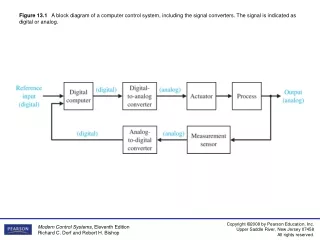
Digital Phase Control System for SSRF LINAC
Digital Phase Control System for SSRF LINAC. C.X. Yin, D.K. Liu, L.Y. Yu SINAP, China. Email: yincx@sinap.ac.cn. Introduction:. As the third synchrotron light source, SSRF contains 150MeV LINAC, 3.5GeV booster and 3.5GeV storage ring. LINAC began to operate on May 2007.

Digital Phase Control System for SSRF LINAC
E N D
Presentation Transcript
Digital Phase Control System for SSRF LINAC C.X. Yin, D.K. Liu, L.Y. Yu SINAP, China Email: yincx@sinap.ac.cn
Introduction: As the third synchrotron light source, SSRF contains 150MeV LINAC, 3.5GeV booster and 3.5GeV storage ring. LINAC began to operate on May 2007. Beam Spot at the end of SSRF LINAC Tunnel of SSRF LINAC
RF phase stability: • When SSRF is operated in top-up mode, LINAC will work in multi-bunch mode. • In order to improve LINAC performance in multi-bunch mode, interpulse phase stability of klystron output should be considered. • Base on the LINAC design, the requirement of RF phase stability is to control interpulse phase shift of klystron output within ±1 degree. So phase control system is implemented in SSRF LINAC.
The design philosophy: • Implement passive coaxial RF component to down-convert RF signal to IF signal, and up-convert IF signal to RF signal. • Implement commercial products for ADC, DAC and clock management modules. • Implement digital I/Q demodulation as phase detecting algorithm, and digital I/Q modulation as phase shifter.
The design philosophy: • Implement feed-forward control to compensate interpulse phase shift of klystron forward signal. • Implement FPGA for signal processing and control. • Implement embedded computer and real-time operation system for iterative algorithm calculation in feed-forward control.
Components in phase control system: • ICS572B: PMC module; two ADCs, two DACs, clock management and FPGA.
Components in phase control system: • GE VMIVME 7050: VME single board computer, used for iterative algorithm calculation. • RF front-end.
RF front-end: • Two klystrons forward signal is down-converted to IF signal (25.6MHz), sampled by two ADCs respectively. • Two DACs outputs are up-converted to RF signal (2997.924MHz), used as power amplifier input. • RF reference signal (2997.924MHz) is down-converted to IF signal (25.6MHz), used as input signal for clock management module in ICS572B.
Clock: • In order to satisfy digital I/Q modulation and demodulation requirement, it is required for sampling clock to be synchronized with reference IF signal. • In conventional design, RF distribution system will provide AD/DA sampling clock that is synchronized with reference IF signal. • In our design, clock management module will provide this function, the complexity of RF distribution system is reduced.
Clock: • Clock management module in ICS572B: TI CDC7005; 409.6MHz VCXO; passive filter for PLL. • Generating 5 clocks which are synchronized with reference IF signal (clock management module input signal). Two ADC sampling clocks (102.4MHz, four times of input signal); Two DAC sampling clocks (204.8MHz, eight times of input signal); One FPGA clock (25.6MHz), used for ADC sampling data alignment.
ADC: • ICS572B includes two 14-bit ADCs (AD6645), and sampling frequency is up to 102.4MHz. • ADC sampling frequency is 102.4MHz in phase control system, and work in simultaneous mode. • Data from two ADCs directly send to FPGA, digital I/Q demodulation is done by FPGA. • Latency for ADC is about 40ns.
DAC: • ICS572B includes two 14-bit DACs (AD9857), and sampling frequency is up to 204.8MHz. • DAC sampling frequency is 204.8MHz in phase control system. • DAC contains digital up-converter, and frequency-tuning value of DDS is set to 1/8 in phase control system. • Two DACs up-convert I/Q data to IF signal (25.6MHz). • FPGA directly send I/Q data to two DACs simultaneously. • Latency for DAC is about 510ns.
Signal processing: • Signal processing includes digital I/Q demodulation, digital I/Q modulation, I/Q to phase conversion, phase to I/Q conversion, and FIR filter. • Digital I/Q modulation is contained in DAC; additional parts are realized in FPGA. • Phase detector (I/Q demodulation) and phase shifter (I/Q modulation) are all realized in digital signal processing mode, so the performance of noise rejection is improved.
Control: • Control includes feed-forward control and iterative algorithm calculation. • Feed-forward control is realized in FPGA, and iterative algorithm calculation is done in software.
FPGA: • FPGA is the key for digital phase control system. • ICS572B contains a Xilinx Virtex-II FPGA (XC2V4000). • In addition to parts of signal processing & control, FPGA contains data format conversion for DAC input, some registers and memory for data exchanging with software. • Close-loop period of phase control system is about 40ns, so the data stream frequency of all parts in FPGA must be more than 25.6MHz.
FPGA: • FPGA contains two identical channels that work simultaneously, one channel controls one klystron forward signal’s phase respectively. Layout of one channel in FPGA
FPGA: • Digital I/Q demodulation: ADC sampling clock is four times of input signal, so digital I/Q can be attained by FPGA clock is used to align four successive sampling data to generate a couple of I/Q data. • FIR filters: 8 taps; used to compensate phase shift between I/Q caused by digital I/Q demodulation algorithm.
FPGA: • CORDIC: 12 taps; used to I/Q to phase conversion and phase to I/Q conversion; the phase conversion accuracy is better than 0.1 degree. • Feed-forward control: the phase difference is attained by comparing reference phase with sampled phase data; the phase of feed-forward control is attained by adding phase difference with feed-forward phase vector in dual port RAM.
FPGA: • 2x1 multiplexer: used to DAC input data conversion; convert parallel I/Q data to interleaved data stream. • The latency of FPGA: 1 period for DDC; 1 period for FIR; 6 periods for CORDIC; 2 periods for feed-forward control; 1 period for 2x1 multiplexer. • The total latency of phase control system is about 1us.
Software: • Iterative algorithm calculation: under VxWorks operation system. • At the end of one pulse, software is triggered by interrupt to read FIFO, which stores all I/Q data in the pulse. • After iterative algorithm calculation, feed-forward phase vector is written to dual port RAM in FPGA.
Preliminary Test: • Tested in LINAC operation condition. • RF reference signal is connected both Kly. A port and RF ref. Port in RF front-end. • Data is acquired by measuring one point phase (2us after trigger rising edge) 1000 times. • The background phase noise is within ±0.6 degree. The background noise of phase control system
Preliminary Test: • Set phase control system in open loop mode. • Data is acquired by measuring interpulse phase and amplitude 1000 times. • Interpulse phase shift is more than 10 degree, phase control system is essential. Interpulse phase of klystron forward signal
Conclusion: • The open-loop test indicated digital phase control system has ability to acquire interpulse phase of klystron output, so the feasibility of our design is proved. • In the background noise test, noise of phase detector is within ±0.6 degree. Because ADC and DAC’s clock source is same, phase noise of close-loop is within 0.1degree (caused by CORDIC). So the total phase noise will be within ±1 degree; the performance of close-loop could be foreseeable.
Conclusion: • Due to the present commissioning stage for SSRF, there is no enough machine study time for LINAC. The close-loop of phase control system will be further tested in future. • This is a helpful reference design for phase control system in next XFEL or CSNS.