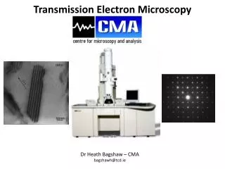
Transmission Electron Microscopy
Transmission Electron Microscopy. Dr Heath Bagshaw – CMA bagshawh@tcd.ie. What is the difference between SEM and TEM?. Scanning Electron Microscope Transmission Electron Microscope. •In an SEM, electrons are scanned over the surface of the sample.

Transmission Electron Microscopy
E N D
Presentation Transcript
Transmission Electron Microscopy Dr Heath Bagshaw – CMA bagshawh@tcd.ie
What is the difference between SEM and TEM? Scanning Electron Microscope Transmission Electron Microscope •In an SEM, electrons are scanned over the surface of the sample. • In a TEM, electrons are transmitted through the sample.
What is a Transmission Electron Microscope (TEM)? •Electrons pass through a (very thin) sample (i.e. are transmitted) to form an image. •Simplistically, In its operation a TEM can be thought of as analogous to a slide projector:- Slide projector Projection screen Objective lens slide Condenser lens TEM Fluorescent screen Light source aperture Specimen (thin) Electron beam Electron source Objective lens Condenser lens
What is a Transmission Electron Microscope (TEM) cont. •In a slide projector white light from the bulb is focussed onto the slide by a condenser lens. •This produces an image which is focussed by the objective lens to a point (crossover). • The image is then projected onto a screen and magnified by varying the distance from the crossover to the screen. •In a TEM the electron beam is focussed on the sample using the condenser lens system. •This produces an image which is focussed by the objective lens to a point (crossover). •This image is then magnified by a series of projector lenses to vary the size of the image on a fluorescent screen. •Changing the current of an electromagnetic lens alters its focal length altering magnification.
Anatomy of a TEM •TEMs’ have basically the same design independent of manufacturer or age:- Electron Gun a) b) c) Condenser lens system Apertures Sample Sample Apertures Viewing Screen Viewing Screen Examples of Transmission Electron Microscopes, a)Philips EM420 (1980s), b) Cut through Schematic of Philips CM 200 (1990s) and c) JEOL 2100 (2000s) • JEOL 2100 has digital imaging and computer assisted operation.
main components of a TEM • The TEM can be broken down into a few main components, these are:- •The Gun – which produces electrons. •The condenser system – which forms the probe. •The sample – sample preparation is important, and time consuming. •Image formation – use of image plane or back focal plane. •Projection of the image (magnification). •Viewing and recording the image. Lets start by looking at how electrons are produced.
Electron Guns •Two main types of gun – Thermionic and Field Emission. •Thermionic sources produce electrons when heated. •Field emission sources produce electrons when exposed to an intense electric field. •FEG’s give much more brightness than thermionic systems. •FEG’s give a more monochromatic electron source and finer probe (i.e. better resolution). Comparison of the three types of source operating at 100kV
The Condenser System •The Wehnelt (or 2nd anode in a FEG) focuses the beam to a crossover which is accelerated down the column. •The first condenser de-magnifies the crossover to give a smaller point source – this is referred to as C1 or spot size. •The second condenser lens (C2) is used to either converge or spread the beam of illumination on the sample (intensity (Philips) or brightness (JEOL)). •A condenser aperture is placed in the beam path to remove electrons far from the optic axis which would reduce resolution. •The smaller the aperture the better the resolution, but there is an associated decrease in brightness – need to compromise.
The Sample •Samples are typically 3mm in diameter and <80µm thick. •Sample preparation is tricky and time consuming. •For a metallic sample:- •Cut\slice a section of material <1mm thick. •Produce 3mm diameter blanks by either Punching, or spark erosion. •Grind and polish blanks to <80µm thick and 0.25µm or better finish. •Either electropolish or, if a light metal Ion Beam mill to perforation – region around the hole should contain electron transparent material (thin area). •For Al based alloys, due to build up of Al2O3 coatings in the presence of air, the samples should be examined immediately after preparation (e.g. prepared in the morning and examined in the afternoon). Thin area
The Sample (2) •For a non metallic sample:- •Cut\slice a section of material <1mm thick. •Mount on glass slide and Grind to <80µm thick with a 0.25µm or better finish. •Mount on support grids if necessary. •Dimple to leave ~10 µm of material remaining. •Ion beam mill to perforation. •Some samples require coating to prevent charging effects. •For powders:- •Grind\mix the powder in chloroform or reagent grade methanol to create a suspension. •Pipette a drop of suspension onto a support grid with a Carbon film coating. •Solvent will evaporate leaving powder dispersed on the grid. •Allow to dry and observe. Biological samples require fixing and embedding before being stained with heavy metals (e.g. OsO4) for contrast prior to ultra microtome sectioning. – Very time consuming.
Focused Ion Beam (FIB) e) •Uses a beam of focused Ga ions to sputter material away. •Fairly new technique (~10-15 years old) which allows site specific micro machining to ‘cut out’ a specific area of a bulk material for TEM analysis. •Usual process is the ‘lift out’ technique, a) to d). •Another common method is the ‘trench milling’ technique, e). • More on this tomorrow...
Image Formation •All rays from a point in the object are gathered by the lens and converge to a point in the image. •All parallel rays are focused in the focal plane. •The back focal plane of the objective lens contains groupings of rays that have left the object at the same angle. •The back focal plane contains the diffraction pattern of the sample. •Diffraction pattern and image are both formed in the imaging process •The intermediate lens is then focused on either the image plane (for the image), or the back focal plane (for the diffraction pattern). sample Objective lens
Imaging Modes •Two principle modes of TEM operation, A – Projecting the diffraction pattern, B – Projecting the image. • The intermediate lens selects either the Back Focal Plane or the image plane of the objective lens.
Contrast •Conventionally, in order to get contrast in an image an objective aperture is placed in the beam path at the back focal plane of the objective lens. •Any electrons which are scattered by interaction with the sample are prevented from recombining in the image by the aperture. •Any regions where electrons are scattered will appear dark in the image. •The smaller the aperture used the greater the contrast, but at the expense of brightness. •Another method of achieving contrast is the ‘Mass thickness Contrast’ mechanism. •Thicker (or higher Z) areas of the sample scatter more electrons than thinner (lower Z areas). •Therefore fewer electrons from the dark region fall onto the screen, so the region appears darker in a Bright Field image. Mechanism of mass thickness contrast
Projection - Magnification •A series of projector lenses are then used to magnify the image formed by the intermediate lens onto a viewing screen. •Electron Microscope lenses are Electro-magnetic in nature. •They consist of a cylindrical soft metal core (polepiece) with a hole drilled through it (bore) wound with copper wire. •When a current is passed through the coils a magnetic field is created in the bore. •Changing the current in the windings changes the magnetic field and effectively changes the focal length of the lens. •Increase the current and the focal length (f) of the lens decreases, so a weaker lens (f1) gives a higher magnification then a stronger lens (f2) as image distance v increases, but the object distance is unchanged.
Viewing\Recording Images •The image, comprising of a beam of focused electrons falls onto a fluorescent screen therefore producing a visible image. •This image can be recorded onto photographic film using the camera located underneath the viewing screen. •Modern machines can capture images digitally using CCD cameras. •The signal from the beam can be output to external analysis equipment, e.g. STEM detectors, EELS etc. for further analysis Fluorescent viewing screen Digital CCD camera
Other analysis Techniques •One of the main strengths of TEM is the ability to obtain diffraction (structural information) and images from the same area at the same time from the same sample from a small volume. •There are, however many more analysis techniques available:- •Energy Dispersive Spectroscopy (EDS) for compositional analysis. •Electron Diffraction – for crystallographic analysis. •Dark Field imaging – enhanced contrast using crystallography. •High Resolution TEM (HRTEM) with resolution to atomic scale. •Scanning TEM (STEM) for increased resolution\contrast. •Electron Energy Loss Spectroscopy (EELS) – to examine local electronic environment allowing mapping of elemental distribution to atomic level. •Tomography – to produce 3 dimensional models of samples. •Low – dose and Cryo TEM to allow analysis of beam sensitive materials e.g. polymers and biological samples.
Energy Dispersive Spectroscopy (EDS) •EDS analysis in the TEM can be performed on very small areas due to very small interaction volume. •In SEM the interaction volume is ~ 1µm3 from a 0.1µm probe size. •In TEM the interaction volume is of the order of nm (~10-8 µm3 for a FEG TEM) due to very thin samples and very small probe sizes. Comparison of interaction volumes in an SEM, Thermionic TEM and FEG TEM showing much smaller interaction volume for TEM.
Electron Diffraction •Diffraction patterns give crystallographic information about a material from site specific small volumes, unlike XRD which is a bulk analysis technique. •Can determine if a material is amorphous, crystalline or poly crystalline quickly and effectively. a)Amorphous material, b) Crystalline material and c) polycrystalline material •Lattice parameter information, unit cell details and any periodicity present in the sample arising from structural transformations or ordering processes can be seen. •Superlattice structure gives information about the long range make up of a material. a) b) c)
SuperLattice Reflections 010 cs 000 001 cs 010 000 001 cs 001 d) cs 0-11 it 000 o2 1-10 o1 000 o1 o1 10-1 at at o1 o2 it it -110 0-11 000 10-1 001 -110 It(ii) at It(i) 000 1-10 at •Patterns a) to c) are electron diffraction patterns taken from CaTiO3 – super lattice reflections are seen showing the presence of Cation Shifts (cs), In-phase tilting (it) and antiphase tilting(at). •Patterns d) to f) are electron diffraction patterns from Sr(Zn1/3)Nb2/3)O3 – the same superlattice reflections are seen as in CaTiO3, but with additional ordering reflections (o1 and o2). •Both CT and SZN have the same tilt system (a-a-c+) so are related, but SZN has long range ordering as well. •CT space group is Pnma (orthorhombic), SZN is P21/c (Monoclinic - β = 125.501°). a) b) c) e) f)
SuperLattice in XRD and ED •In XRD traces the appearance of superlattice reflections is influenced by the size difference of the cations. Major perovskite reflection •The ordering peak (~20° 2 Theta) in SMN is much larger (Approx. 12X) than the same peak in SZN. ½(hk0)In phase tilting reflection •Consequently, the ordering peak in SZN is easy to overlook. • This is not a problem in Electron Diffraction. <111> electron diffraction pattern of CT Major perovskite reflection ½(hkl)anti phase tilting reflection 1/3(hkl)ordering reflection <110> electron diffraction pattern of SMN Ordering Peak Intensity Intensity •Superlatticereflections are clearly visible in electron diffraction patterns. •Electron diffraction therefore provides a powerful tool for the investigation of superlattice reflections in materials (e.g. Tilting, ordering and layered structures). °2Theta °2Theta SMN ordering peak in XRD SZN ordering peak in XRD
Symmetry Analysis •Convergent Beam Electron Diffraction (CBED) is a powerful tool for analysing and identifying symmetry in materials. •a)Convergent Beam Electron Diffraction (CBED) pattern showing Six fold rotational symmetry and b)Selected area Diffraction Pattern (SADP) of same area. •Unknown materials can be analysed and their space groups be found to aid identification\characterisation. a) b)
Symmetry Analysis 2 •Overlaying of CBED patterns gives a map of the crystal which you can navigate around to find the region\ zone axis (direction) of interest. •Overlayed CBED patterns for a FCC system. <111> <110> <100>
Dark Field Imaging •Dark Field images are formed from specific diffracted beams, giving orientation contrast. •Bright Field images are formed using spot A. •A typical Dark Field images would be formed using spot B. •Bright field images contain information from all electrons that have passed through the sample therefore subtle features are hidden. •With Dark Field images, a specific plane can be viewed in order to see specific crystallographic features such as dislocations, regions of ordering or strain fields etc. •Dark field images typically have considerably higher contrast than bright field images although the intensity is greatly reduced.
Dark Field Image formation • Can select the spot by moving the aperture or tilting the beam to bring the selected spot to the optical axis of the microscope. Image formation for a Bright Field, Displaced Aperture Dark Field (DADF) and Centred Aperture Dark Field (CADF) image.
Dark Field Imaging Example 1.0 μm 1.0 μm c) d) 001 010 at 000 110 000 10-1 cs a) b) •Image a) illuminated with Cation Shift (cs) spot in c). •Image b) illuminated with Antiphase tilt (at) spot in d). •c) and d) both <110> zone axis diffraction patterns (ZADP). •Clear crystallographic difference between the two area is seen visually.
Dark Field Imaging Example 2 300nm b) a) •Image a) Dark Field image of unshadowed and unstained DNA, Image b) illuminated with ordering superlattice reflection – regions of ordering clearly visible.
Dark Field – Advantages and Disadvantages •Advantages and disadvantages of Dark Field Imaging :- •Advantages •Provides high contrast for examining molecules with very low contrast such as DNA. •For crystalline objects, specific diffraction spots can be selected in the back focal plane of the objective lens in order to form a dark field image only from the electrons scattered by a chosen set of crystal planes. •Disadvantages •More difficult to focus and correct for astigmatism since phase contrast is not present. •Image brightness is low, since the objective aperture transmits only a small fraction of the scattered beam,, •Longer exposure times needed to get good photographic images. •Consequently, specimens are subjected to greater levels of radiation damage.
High Resolution TEM (HRTEM) •High resolution TEM images are formed by a process known as phase contrast. •Contrast is formed by constructive or destructive interference between electron wave passing through a material. •No objective aperture is used. •The appearance of the image can change by altering the focus. •Perfect focus is known as ‘Scherzer defocus’ – all electron waves are in phase – no contrast. •As focus is altered (either de-focused or over focused) the waves move out of phase giving rise to interference patterns. •These ‘patterns’ form the actual image. •Image simulations are then needed to verify interpretation on the image recorded – very involved.
High Resolution TEM Examples HR 500kV lattice fringe image of ‘as grown’ silicon on sapphire showing complex twinning and stacking defects Structure image of <100> tilt grain boundary in nickel oxide. Images from ‘HRTEM and associated techniques –Buseck, Cowley and Eyring – Oxford science pub
High Resolution TEM – Image Simulation Simulated HRTEM images showing how features change as the focus changes (Δf).
Scanning TEM (STEM) •In conventional TEM imaging an objective aperture is used to select the transmitted or scattered beam in order to select the source of contrast. •In STEM the transmitted or scattered beam is selected in an equivalent way by using detectors rather than apertures. •Comparison of the use of an objective aperture in TEM to select the transmitted or scattered beam forming BF or DF image respectively •In STEM an on-axis, or annular detector is used to perform equivalent operations.
Why use STEM? •For DF imaging the annular detector collects more electrons than an aperture. •STEM ADF images are less noisy then TEM DF images as no lenses are used to form them. •Contrast in STEM images is greater than standard DF images. a) b) c) • Comparison of TEM DF and STEM ADF images of the same sample shows clear contrast difference • The low contrast in the TEM image (a) is enhanced in the STEM image (b) by signal processing. • Image c) is a digitised TEM DF image treated with contrast enhancement software.
EELS •Electron Energy Loss Spectroscopy. •As electrons interact with matter they lose energy to it. •A magnetic prism disperses these electrons according to energy, then a spectrometer located at the correct position can collect electrons of a specific energy. •Can not only detect positions of individual atoms, but also the oxidation state.
EELS - Examples •Typical EELS spectrum showing absorption edges for three different elements, different oxidation states give different shaped ‘edges’, takes experience to analyse properly. •Elemental distribution maps for C, Ti, O and Cu , maps taken by filtering particular edges. •Can clearly see atomic distribution at nm scale.
Tomography •Sample rotated through large angles in the electron beam and photos taken at each angle. •Powerful computers then used to render 3D model. •Very time consuming process, automation software such as Leginon* is often used for image capture process. *(The Scripps Research Institute – Journal of Structural Biology, Vol 151, Issue 1, P 41-60)
Cryo TEM •To reduce damage to sensitive organic samples (biological\polymeric) Cryo TEM technique is used. •Samples are prepared and analysed at low temperatures (usually liquid Nitrogen -196⁰C) to minimise heating effect of electron beam. Longitudinal section through rat ventricular myocytes. A- Nucleus, B- Z-Line, C- A- Band and D – Mitochondria* *Dept Cellular Sciences – emlab.ubc.ca – www.emlab.ubc.ca/sub/gallery.html
Conclusions •TEM is a very versatile analysis technique. •Many different types of analysis can be performed (hardware dependent). •Complimentary information can be obtained from distinct small (nm) regions allowing full nano-scale characterisation. •Sample preparation is very time consuming requiring expertise to get the right results. •Sampling ratio is poor – the sample is 3mm in diameter and ~ 80-100µm thick – is this really representative of the sample ?– have to assume it is. •Future improvements, such as aberration correctors and monochromators will give finer control of probe sizes leading to higher resolution.
ED example - Perovskites •The prototype perovskite structure with general formula ABO3 can be described as a cubic arrangement of corner-shared BO6 anion octahedra enclosing a single A-site cubooctahedralcation arranged within a three dimensional O2- network. •The perovskite structure is able to sustain a wide range of cation sizes for both the A and B sites. •The most well known perovskite is BaTiO3 although the name derives from CaTiO3. •The most common phase transitions in perovskites involve rotation, or tilting, of the corner shared octahedra making up the structure. The cubic unit cell of BaTiO3 •This results in a doubling of the unit cell and gives rise to a reflection in reciprocal space at a ½ integer position. Schematic diagram illustrating octahedral tilting around an axis perpendicular to the paper.