Field Effect Transistors (FET)
Field Effect Transistors (FET). Enhancement/ Depletion Current vs Voltage Characteristics DC/ Small Signal Analysis. Chapter 4, FET Transistors due Sep. 24 4.12,4.46,4.75,4.96 Quiz 1 Sep 28 Quiz 2 Oct 30 Project abstracts due October 9 (Tuesday following Monday schedule).

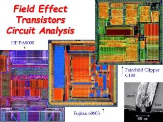
Field Effect Transistors (FET)
E N D
Presentation Transcript
Field Effect Transistors (FET) Enhancement/ Depletion Current vs Voltage Characteristics DC/ Small Signal Analysis September 17, 2007
Chapter 4, FET Transistors due Sep. 24 4.12,4.46,4.75,4.96 Quiz 1 Sep 28 Quiz 2 Oct 30 Project abstracts due October 9 (Tuesday following Monday schedule) HW & Project September 17, 2007
Field Effect (MOS) Transistor Typically L = 1 to 10 m, W = 2 to 500 m, and the thickness of the oxide layer is in the range of 0.02 to 0.1 m. September 17, 2007
Operation The enhancement-type NMOS transistor with a positive voltage applied to the gate. An n channel is induced at the top of the substrate beneath the gate. September 17, 2007
Triode Region vGS > Vt ,small vDS applied. the channel conductance is proportional to vGS - Vt, and is proportional to (vGS - Vt) vDS. September 17, 2007
Saturation Region vGS > Vt. The induced channel acquires a tapered shape and its resistance increases as vDS is increased. September 17, 2007
Drain current iD versus vDS Enhancement-type NMOS transistor operated with vGS > Vt. September 17, 2007
Derivation of the iD - vDS characteristic of the NMOS transistor. September 17, 2007
Cross section of a CMOS integrated circuit. Note that the PMOS transistor is formed in a separate n-type region, known as an n well. Another arrangement is also possible in which an n-type body is used and the n device is formed in a p well. September 17, 2007
n-channel enhancement-type MOSFET with vGSand vDSapplied and with the normal directions of current flow The iD - vDS characteristics for a device with Vt = 1 V and k’n(W/L) = 0.5 mA/V2. September 17, 2007
iD - vGS characteristic for an enhancement-type NMOS transistor in saturation (Vt = 1 V and k’n(W/L) = 0.5 mA/V2). September 17, 2007
Increasing vDSbeyond vDSsat causes the channel pinch-off point to move slightly away from the drain, thus reducing the effective channel length (by L). September 17, 2007
Effect of vDS on iD in the saturation region. The MOSFET parameter VAis typically in the range of 30 to 200 V. September 17, 2007
Large-signal equivalent circuit model • n-channel MOSFET in saturation, incorporating the output resistance ro. • The output resistance roVA/ID. September 17, 2007
The current-voltage characteristics of a depletion-type n-channel MOSFET for which Vt = -4 V and k’n(W/L) = 2 mA/V2 iD - vGS saturation September 17, 2007 iD - vDS characteristics
MOSFET as an amplifier. September 17, 2007
Small Signal Instantaneous voltages vGSand vD September 17, 2007
Models for MOSFET neglecting the dependence of iD on vDS in saturation (channel-length modulation effect) September 17, 2007
Model with Output Resistance Including the effect of channel-length modulation modeled by output resistance ro = |VA|/ID. September 17, 2007
T model of the MOSFET T model of the MOSFET augmented with the drain-to-source resistance ro. September 17, 2007
Sample Circuit Output characteristic of the current current mirror Q2 is matched to Q1. MOSFET current mirror. September 17, 2007
The CMOS common-source amplifier September 17, 2007
The CMOS common-gate amplifier September 17, 2007
The source follower • circuit; • small-signal equivalent circuit • simplified version of the equivalent circuit. September 17, 2007
NMOS amplifier with enhancement load graphical determination of the transfer characteristic transfer characteristic. September 17, 2007
The NMOS amplifier with depletion load: (a) circuit; (b) graphical construction to determine the transfer characteristic; and (c) transfer characteristic. September 17, 2007
Small-signal equivalent circuit of the depletion-load amplifier With the body effect of Q2. September 17, 2007
The CMOS inverter Simplified circuit schematic for the inverter. September 17, 2007
CMOS inverter operation v1 is high: (a) circuit with v1 = VDD (logic-1 level, or VOH); (b) graphical construction to determine the operating point; and (c) equivalent circuit. September 17, 2007
CMOS inverter operation v1 is low: graphical construction to determine the operating point; and (c) equivalent circuit. September 17, 2007
Voltage transfer characteristic of the CMOS inverter. September 17, 2007