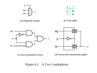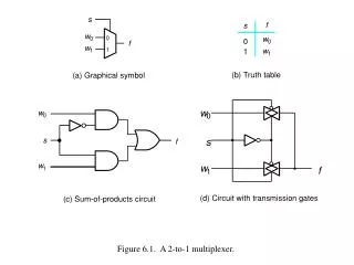
Figure 6.1. A 2-to-1 multiplexer.
660 likes | 1.17k Vues
s. f. s. w. w. 0. 0. 0. 0. f. w. 1. w. 1. 1. 1. (b) Truth table. (a) Graphical symbol. w. w. 0. 0. s. s. f. w. w. f. 1. 1. (d) Circuit with transmission gates. (c) Sum-of-products circuit. Figure 6.1. A 2-to-1 multiplexer. s. 0. s. s. s. f. 1. 1. 0. w.

Figure 6.1. A 2-to-1 multiplexer.
E N D
Presentation Transcript
s f s w w 0 0 0 0 f w 1 w 1 1 1 (b) Truth table (a) Graphical symbol w w 0 0 s s f w w f 1 1 (d) Circuit with transmission gates (c) Sum-of-products circuit Figure 6.1. A 2-to-1 multiplexer.
s 0 s s s f 1 1 0 w w 00 0 0 0 0 w 01 w 1 0 1 f 1 w 10 w 2 1 0 2 w 11 3 w 1 1 3 (a) Graphic symbol (b) Truth table s 0 w 0 s 1 w 1 f w 2 w 3 (c) Circuit Figure 6.2. A 4-to-1 multiplexer.
s 1 s 0 w 0 0 w 1 1 0 f 1 w 0 2 w 1 3 Figure 6.3. Using 2-to-1 multiplexers to build a 4-to-1 multiplexer.
s 0 s 1 w 0 w 3 s w 2 4 s 3 w 7 f w 8 w 11 w 12 w 15 Figure 6.4. A 16-to-1 multiplexer.
s x y 1 1 x y 2 2 (a) A 2x2 crossbar switch x 0 1 y 1 1 s x 0 2 y 2 1 (b) Implementation using multiplexers Figure 6.5. A practical application of multiplexers.
Please see “portrait orientation” PowerPoint file for Chapter 6 Figure 6.6. Implementing programmable switches in an FPGA.
w w w f 2 1 2 w 1 0 0 0 0 1 0 1 1 f 1 1 0 1 0 0 1 1 (a) Implementation using a 4-to-1 multiplexer w w f 1 2 f w 1 w 1 0 0 0 w 0 2 1 0 1 w w 1 2 2 1 1 0 f 0 1 1 (c) Circuit (b) Modified truth table Figure 6.7. Synthesis of a logic function using multiplexers.
w w w f 1 2 3 w w f 1 2 0 0 0 0 0 0 0 0 0 1 0 w 0 1 3 0 1 0 0 w 1 0 3 0 1 1 1 1 1 1 1 0 0 0 1 0 1 1 1 1 0 1 1 1 1 1 (a) Modified truth table w 2 w 1 0 w 3 f 1 (b) Circuit Figure 6.8. Three-input majority function.
w w w f 1 2 3 0 0 0 0 0 0 1 1 w Å w w 2 2 3 w 0 1 0 1 1 w 0 1 1 0 3 1 0 0 1 f 1 0 1 0 Å w w 2 3 1 1 0 0 1 1 1 1 (a) Truth table (b) Circuit Figure 6.9. Three-input XOR function implemented with 2-to-1 multiplexers.
w w w f 1 2 3 0 0 0 0 w 3 w 0 0 1 1 2 w 1 0 1 0 1 w 3 w 0 1 1 0 3 1 0 0 1 f w 3 1 0 1 0 1 1 0 0 w 3 1 1 1 1 (b) Circuit (a) Truth table Figure 6.10. Three-input XOR function implemented with a 4-to-1 multiplexer.
w w w f 1 2 3 f 0 0 0 0 w 1 0 0 1 0 w w 0 2 3 0 1 0 0 w + w 1 2 3 0 1 1 1 1 0 0 0 1 0 1 1 1 1 0 1 1 1 1 1 (b) Truth table w 1 w 2 w 3 f (b) Circuit Figure 6.11. Three-input majority function implemented using a 2-to-1 multiplexer.
w w 2 1 0 w 3 f 1 Figure 6.13. Example circuit.
w 1 0 f w 1 w f 2 w 3 f w 1 w 4 (a) Using three 3-LUTs w 2 0 w f f 1 w 2 w 3 w 4 (b) Using two 3-LUTs Figure 6.14. Example circuits.
w y 0 0 n n 2 inputs w outputs n – 1 y n Enable 2 – 1 En Figure 6.15. An n-to-2n binary decoder.
w w y y y y En 1 0 0 1 2 3 w y 0 0 0 0 0 1 0 0 1 w y 1 1 0 1 0 1 0 0 1 y 2 1 1 0 0 0 1 0 y En 3 1 1 1 0 0 0 1 x x 0 0 0 0 0 (a) Truth table (b) Graphical symbol w 0 y 0 w 1 y 1 y 2 y 3 En (c) Logic circuit Figure 6.16. A 2-to-4 decoder.
w y w y 0 0 0 0 w y w y 1 1 1 1 y y 2 2 w y 2 y En 3 3 y w y En 4 0 0 y w y 5 1 1 y y 6 2 y y En 7 3 Figure 6.17. A 3-to-8 decoder using two 2-to-4 decoders.
w y w y 0 0 0 0 w y w y 1 1 1 1 y y 2 2 y y En 3 3 y w y 4 0 0 w y y 5 1 1 y y 2 6 w w y y y 2 En 0 0 3 7 w w y 3 1 1 y 2 y w y y En En 8 0 0 3 y w y 9 1 1 y y 2 10 y y En 3 11 y w y 12 0 0 y w y 13 1 1 y y 2 14 y y En 3 15 Figure 6.18. A 4-to-16 decoder built using a decoder tree.
w 0 w 1 s w y 0 0 0 s w y f 1 1 1 y w 2 2 y En 1 3 w 3 Figure 6.19. A 4-to-1 multiplexer built using a decoder.
w 0 s w y w 0 0 0 1 s w y 1 1 1 f y 2 y En 1 3 w 2 w 3 Figure 6.20. A 4-to-1 multiplexer built using a decoder and tri-state buffers.
Sel 0 0/1 0/1 0/1 Sel 1 0/1 0/1 0/1 Sel a 2 0 0/1 0/1 0/1 decoder a 1 Address m -to-2 a m – 1 m Sel m 2 – 1 0/1 0/1 0/1 Read d d d Data n – 1 n – 2 0 Figure 6.21. A 2m x n read-only memory (ROM) block.
w 0 y 0 n n 2 outputs inputs y n – 1 w n 2 – 1 Figure 6.22. A 2n-to-n binary encoder.
w w w w y y 3 2 1 0 1 0 0 0 0 1 0 0 0 0 1 0 0 1 0 1 0 0 1 0 1 0 0 1 1 0 (a) Truth table w 0 w 1 y 0 w 2 y 1 w 3 (b) Circuit Figure 6.23. A 4-to-2 binary encoder.
w w w w y y z 3 2 1 0 1 0 0 0 0 0 d d 0 0 0 0 1 0 0 1 x 0 0 1 0 1 1 x x 0 1 1 0 1 x x x 1 1 1 1 Figure 6.24. Truth table for a 4-to-2 priority encoder.
a a b w f b 0 c w 1 d w g 2 e e c w 3 f d g (a) Code converter (b) 7-segment display c e g w w w w a b d f 3 2 1 0 0 0 0 0 1 1 1 1 1 1 0 0 0 0 1 0 1 1 0 0 0 0 0 0 1 0 1 1 0 1 1 0 1 0 0 1 1 1 1 1 1 0 0 1 0 1 0 0 0 1 1 0 0 1 1 0 1 0 1 1 0 1 1 0 1 1 0 1 1 0 1 0 1 1 1 1 1 1 1 1 0 1 1 1 0 0 0 0 1 1 1 1 1 1 1 1 0 0 0 1 0 0 1 1 1 1 1 0 1 1 (c) Truth table Figure 6.25. A BCD-to-7-segment display code converter.
module mux2to1 (w0, w1, s, f); input w0, w1, s; output f; assign f = s ? w1 : w0; endmodule Figure 6.27. A 2-to-1 multiplexer specified using the conditional operator.
module mux2to1 (w0, w1, s, f); input w0, w1, s; output f; reg f; always @(w0 or w1 or s) f = s ? w1 : w0; endmodule Figure 6.28. An alternative specification of a 2-to-1 multiplexer using the conditional operator.
module mux4to1 (w0, w1, w2, w3, S, f); input w0, w1, w2, w3; input [1:0] S; output f; assign f = S[1] ? (S[0] ? w3 : w2) : (S[0] ? w1 : w0); endmodule Figure 6.29. A 4-to-1 multiplexer specified using the conditional operator.
module mux2to1 (w0, w1, s, f); input w0, w1, s; output f; reg f; always @(w0 or w1 or s) if (s==0) f = w0; else f = w1; endmodule Figure 6.30. Code for a 2-to-1 multiplexer using the if-else statement.
module mux4to1 (w0, w1, w2, w3, S, f); input w0, w1, w2, w3; input [1:0] S; output f; reg f; always @(w0 or w1 or w2 or w3 or S) if (S == 2'b00) f = w0; elseif (S == 2'b01) f = w1; elseif (S == 2'b10) f = w2; elseif (S == 2'b11) f = w3; endmodule Figure 6.31. Code for a 4-to-1 multiplexer using the if-else statement.
module mux4to1 (W, S, f); input [0:3] W; input [1:0] S; output f; reg f; always @(W or S) if (S == 0) f = W[0]; else if (S == 1) f = W[1]; else if (S == 2) f = W[2]; else if (S == 3) f = W[3]; endmodule Figure 6.32. Alternative specification of a 4-to-1 multiplexer.
module mux16to1 (W, S16, f); input [0:15] W; input [3:0] S16; output f; wire [0:3] M; mux4to1 Mux1 (W[0:3], S16[1:0], M[0]); mux4to1 Mux2 (W[4:7], S16[1:0], M[1]); mux4to1 Mux3 (W[8:11], S16[1:0], M[2]); mux4to1 Mux4 (W[12:15], S16[1:0], M[3]); mux4to1 Mux5 (M[0:3], S16[3:2], f); endmodule Figure 6.33. Hierarchical code for a 16-to-1 multiplexer.
module mux4to1 (W, S, f); input [0:3] W; input [1:0] S; output f; reg f; always @(W or S) case (S) 0: f = W[0]; 1: f = W[1]; 2: f = W[2]; 3: f = W[3]; endcase endmodule Figure 6.34. A 4-to-1 multiplexer defined using the case statement.
module dec2to4 (W, Y, En); input [1:0] W; input En; output [0:3] Y; reg [0:3] Y; always @(W or En) case ({En, W}) 3'b100: Y = 4'b1000; 3'b101: Y = 4'b0100; 3'b110: Y = 4'b0010; 3'b111: Y = 4'b0001; default: Y = 4'b0000; endcase endmodule Figure 6.35. Verilog code for a 2-to-4 binary decoder.
module dec2to4 (W, Y, En); input [1:0] W; input En; output [0:3] Y; reg [0:3] Y; always @(W or En) begin if (En == 0) Y = 4'b0000; else case (W) 0: Y = 4'b1000; 1: Y = 4'b0100; 2: Y = 4'b0010; 3: Y = 4'b0001; endcase end endmodule Figure 6.36. Alternative code for a 2-to4 binary decoder.
module dec4to16 (W, Y, En); input [3:0] W; input En; output [0:15] Y; wire [0:3] M; dec2to4 Dec1 (W[3:2], M[0:3], En); dec2to4 Dec2 (W[1:0], Y[0:3], M[0]); dec2to4 Dec3 (W[1:0], Y[4:7], M[1]); dec2to4 Dec4 (W[1:0], Y[8:11], M[2]); dec2to4 Dec5 (W[1:0], Y[12:15], M[3]); endmodule Figure 6.37. Verilog code for a 4-to-16 decoder.
module seg7 (bcd, leds); input [3:0] bcd; output [1:7] leds; reg [1:7] leds; always @(bcd) case (bcd) //abcdefg 0: leds = 7'b1111110; 1: leds = 7'b0110000; 2: leds = 7'b1101101; 3: leds = 7'b1111001; 4: leds = 7'b0110011; 5: leds = 7'b1011011; 6: leds = 7'b1011111; 7: leds = 7'b1110000; 8: leds = 7'b1111111; 9: leds = 7'b1111011; default: leds = 7'bx; endcase endmodule Figure 6.38. Code for a BCD-to-7-segment decoder.
// 74381 ALU module alu(s, A, B, F); input [2:0] s; input [3:0] A, B; output [3:0] F; reg [3:0] F; always @(s or A or B) case (s) 0: F = 4'b0000; 1: F = B - A; 2: F = A - B; 3: F = A + B; 4: F = A ^ B; 5: F = A | B; 6: F = A & B; 7: F = 4'b1111; endcase endmodule Figure 6.39. Code that represents the functionality of the 74381 ALU chip.
module priority (W, Y, z); input [3:0] W; output [1:0] Y; output z; reg [1:0] Y; reg z; always @(W) begin z = 1; casex(W) 4'b1xxx: Y = 3; 4'b01xx: Y = 2; 4'b001x: Y = 1; 4'b0001: Y = 0; default: begin z = 0; Y = 2'bx; end endcase end endmodule Figure 6.41. Verilog code for a priority encoder.
module dec2to4 (W, Y, En); input [1:0] W; input En; output [0:3] Y; reg [0:3] Y; integer k; always @(W or En) for (k = 0; k <= 3; k = k+1) if ((W == k) && (En == 1)) Y[k] = 1; else Y[k] = 0; endmodule Figure 6.42. A 2-to-4 binary decoder specified using the for loop.
module priority (W, Y, z); input [3:0] W; output [1:0] Y; output z; reg [1:0] Y; reg z; integer k; always @(W) begin Y = 2'bx; z = 0; for (k = 0; k < 4; k = k+1) if(W[k]) begin Y = k; z = 1; end end endmodule Figure 6.43. A priority encoder specified using the for loop.
Please see “portrait orientation” PowerPoint file for Chapter 6 Table 6.2. Verilog operators.
& 0 1 x j 0 1 x 0 0 0 0 0 0 1 x 1 0 1 x 1 1 1 1 x 0 x x x x 1 x ^ 0 1 x ~^ 0 1 x 0 0 1 x 0 1 0 x 1 1 0 x 1 0 1 x x x x x x x x x Figure 6.44. Truth tables for bitwise operators.
module compare (A, B, AeqB, AgtB, AltB); input [3:0] A, B; output AeqB, AgtB, AltB; reg AeqB, AgtB, AltB; always @(A or B) begin AeqB = 0; AgtB = 0; AltB = 0; if(A == B) AeqB = 1; else if (A > B) AgtB = 1; else AltB = 1; end endmodule Figure 6.45. Verilog code for a four-bit comparator.
module addern (carryin, X, Y, S, carryout); parameter n=32; input carryin; input [n-1:0] X, Y; output [n-1:0] S; output carryout; wire [n:0] C; genvar k; assign C[0] = carryin; assign carryout = C[n]; generate for (k = 0; k < n; k = k+1) begin: fulladd_stage wire z1, z2, z3; //wires within full-adder xor (S[k], X[k], Y[k], C[k]); and (z1, X[k], Y[k]); and (z2, X[k], C[k]); and (z3, Y[k], C[k]); or (C[k+1], z1, z2, z3); end endgenerate endmodule Figure 6.46. Using the generate loop to define an n-bit ripple-carry adder.
module mux16to1 (W, S16, f); input [0:15] W; input [3:0] S16; output f; reg f; always @(W or S16) case (S16[3:2]) 0: mux4to1(W[0:3], S16[1:0], f); 1: mux4to1(W[4:7], S16[1:0], f); 2: mux4to1(W[8:11], S16[1:0], f); 3: mux4to1(W[12:15], S16[1:0], f); endcase // Task that specifies a 4-to-1 multiplexer task mux4to1; input [0:3] X; input [1:0] S4; output g; reg g; case (S4) 0: g = X[0]; 1: g = X[1]; 2: g = X[2]; 3: g = X[3]; endcase endtask endmodule Figure 6.47. Use of a task in Verilog code.