Microelectronics 2
Electrical Engineering 2. Microelectronics 2 . Dr. Peter Ewen. (Room G08, SMC; email - pjse). ELECTRICAL ENGINEERING 2 Microelectronics 2 Dr. P.J.S. Ewen. LECTURES: Mondays 12.10-13.00 Swann 7.20 Fridays 10.00-10.50 JCMB 5327. TUTORIALS: Mondays 11.10-12.00 Eng. CR 4

Microelectronics 2
E N D
Presentation Transcript
Electrical Engineering 2 Microelectronics 2 Dr. Peter Ewen (Room G08, SMC; email - pjse)
ELECTRICAL ENGINEERING 2 Microelectronics 2 Dr. P.J.S. Ewen LECTURES: Mondays 12.10-13.00 Swann 7.20 Fridays 10.00-10.50 JCMB 5327 TUTORIALS: Mondays 11.10-12.00 Eng. CR 4 Tuesdays 11.10-12.00 Eng. CR 4 N.B. Tutorials run in weeks 3, 5, 7, 9, 11
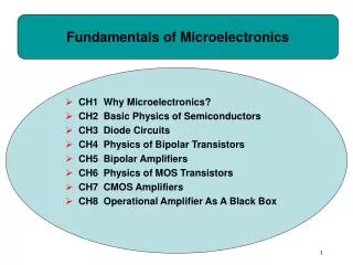
Microelectronics 2 Lecture Topics • Structure and fabrication • Principles of operation • Properties • Applications LECTURES 1-6 Semiconductor theory Basic semiconductor properties: e.g. energy bands, carrier concentrations, mobility, conductivity LECTURES 7-12 Fabrication & p-n junctions LECTURES 13-17 Field Effect Transistors LECTURES 18-20 Bipolar Junction Transistors
The handout contains additional explanatory notes as well as the Powerpoint slides – this additional information generally appears in a pane headed Notes to the right of the corresponding slide.
Recommended text • T.F. Bogart “Electronic • Devices and Circuits” Microelectronics 2 • Formula sheet • Issued with exam paper • Powerpoint slides • Slides available on web – follow link on “Microelectronics 2” LEARN page: Resources also include lecture examples, tutorial solutions, etc.
LECTURE 1 • Importance of semiconductor devices • Device miniaturization • Revision of basic concepts: Resistance and resistivity Conductance and conductivity Electric field Energy of a charged particle
300 250 200 150 100 50 0 3.0 2.5 2.0 1.5 1.0 0.5 0 Electronics is America’s Largest Industry Jobs Industry shipments Shipments ($billions) Jobs (millions) Steel mill products Aerospace Electronics Motor vehicles and parts Fig. 1a
Fig. 1b How the different electronics industries contribute to the overall totals The semiconductor industry underpins all the other electronics industries
105 104 103 102 101 GWP Electronics Automobiles Global sales ($ Billions) Semi- conductors Steel Source: “Fundamentals of semiconductor Fabrication” by G.S. May and S.M. Sze 1980 1990 2000 2010 Year Fig. 2 Gross world product (GWP) and sales volumes of various manufacturing industries from 1980 to 2000 and projected to 2010.
The UK Electronics Industry • Annual sales – £23 billion • Employs 250,000 people • 8000+ electronics companies • 5th largest in the world in terms of production • Accounts for 6% of UK manufacturing output & 2.5% of UK’s GDP • 40% of Europe’s semiconductor design revenue comes from UK • Electronics overtook whisky as Scotland’s No.1 export in the early 1980’s Sources: IET Holyrood Briefings Dec. 2008 Innovation UK 2008 National Microelectronics Institute – sector information
The UK Semiconductor Industry • Employs 4,700 • £4.5 billion revenue • 13 semiconductor manufacturing plants • 19.6% of Europe’s semiconductor market share • Semiconductor fabrication companies in Scotland include: Sources: ICAF Industry study 2007 Hansard 2008
The Scottish Microelectronics Centre (SMC) • Part of the School of Engineering • Located at west end of the KB site • Contains >£10M of equipment dedicated to making IC’s
The Scottish Microelectronics Centre Wet etching bench Access corridor to the 8 cleanroom bays Lithography area
Jack Kilby wins 2000 Nobel Prize for Physics • Jack Kilby received his B.Sc. in Electrical Engineering from the University of Illinois in 1947. • Won the 2000 Nobel Prize in Physics for his part in the invention and development of the integrated circuit. • Kilby invented the IC in 1958 while at Texas Instruments.
Jack Kilby wins 2000 Nobel Prize for Physics • The Nobel citation says: • “…Kilby’s invention enabled the microelectronics field to grow to become the basis of all modern technology.”
Spot the difference… Walter Brattain, William Shockley and John Bardeen – inventors of the transistor, for which they were awarded the Nobel Prize for Physics in 1956. Larry, Curly and Mo – the Three Stooges – a well-known comedy trio of the 1950’s.
1 cm On 16th December 1947 the first transistor was demonstrated – it was a germanium point-contact device. Au (emitter) Au (collector) Ge (base) Fig. 3
How many transistors (approximately) are there in the latest Intel microprocessor chip? 1 - 30,000 2 - 300,000 3 - 3 million 4 - 30 million 5 - 300 million 6 - 3 billion Latest Intel processor “Ivy Bridge” – May 2011
22 nm How big, approximately, is 22nm? (1nm = 10-9m) 1 - Size of a red blood cell 2 - Width of a human hair 3 - Size of a staphylococcus bacterium 4 - Width of a DNA molecule 5 - 90 silicon atoms side by side 6 - Size of a cold virus
90,000nm 600nm 6,000nm 500nm hair red blood cell staphylococcus bacterium atoms in a silicon crystal DNA molecule cold virus 20nm 5nm – 20 atoms 2nm
gate drain source d T L n-type Si n-type Si p-type Si wafer MOS Transistor L T d Fig. 4
Gordon E. Moore, co-founder of Intel. “Moore’s Law” – The number of transistors per chip (die) doubles approximately every 18 months. Fig. 5
World’s Smallest Practical Transistor drain gate source Fig. 6
REASONS FOR CONTINUING SIZE REDUCTION • Higher productivity • Faster operation • Lower power consumption • Higher yield • New products
(a) 52 possible IC’s but only 40 are defect-free Yield = 40/52 = 77% Defects By making the IC’s smaller, more of them manage to avoid the defect sites. (b) 240 possible IC’s but only 224 are defect-free Yield = 224/240 = 93% Fig. 7
Resistance and Resistivity Cross-sectional area A A = ab A = r2 R = ρl/A A = ? a l b r l ρ is Resistivity – depends only on the material l A Fig. 8: The resistance of an object with uniform cross-sectional area A. R is Resistance – depends on the material and geometry of the object
CONDUCTANCE G = 1/R CONDUCTIVITY σ = 1/ρ
Lecture Examples 1. Resistance The figure shows a composite block consisting of a copper cylinder embedded in a stainless steel bar of square cross-section. Calculate the resistance between the opposite ends of the block if the conductivities are: σCu = 5.7x10⁷ Sm-1 σs.s. = 106 Sm-1
1. Resistance The copper cylinder can be represented by a resistor R1... and the stainless R2 steel surrounding it by a resistor R2: R1 R1 and R2 are in parallel, so the total resistance between the ends will be given by: σCu = 5.7x10⁷ Sm-1 σs.s. = 106 Sm-1 σ = 1/ρ
ELECTRIC FIELD + Fig. 9 E F F + - F = qEE is Electric Field F is Force on Charge q Direction of the Electric Field is defined by the direction of the force on a positive charge – i.e. if q is positive, F and E are in the same direction. V is Potential Units for E: Vm-1 for V = kx + C
ΔV |E| = Δx ΔV Fig. 10 +ve -ve E Δx Fig. 11 Δx +ve ΔV E -ve
2. Electric field A Cu wire (ρCu = 1.7x10⁻⁸ Ωm) is joined to an Fe wire (ρFe = 1x10⁻⁷ Ωm). If both wires are 10 m long and have the same radius, calculate the field in each wire if the voltage across the ends is 100 V.
2. Electric Field ΔV |E| = Δx 100 V Cu Fe 10m 10m ρFe = 1x10⁻⁷ Ωm ρCu = 1.7x10⁻⁸ Ωm RFe RCu ΔVCu ΔVFe The two wires can be regarded as two resistors in series, RCu and RFE , with voltage differences ΔVCu and ΔVFe across them. The two resistors in series, RCu and RFE , form a voltage divider, so: R = ρl/A
ΔV |E| = Δx 2. Electric Field 100 V Cu Fe ρFe = 1x10⁻⁷ Ωm ρCu = 1.7x10⁻⁸ Ωm RCu RFe ΔVCu ΔVFe 14.5V
Energy acquired by a charge, q, moving through a potential difference, ΔV V1 ΔV = V2 – V1 V2 q Δx Fig. 12 Energy (Work) = Force × Distance = qE ×Δx = q ×Δx = q ΔV ΔV Δx If q and ΔV are both positive, the change in the energy of the particle will be positive, i.e. its energy will increase.
SUMMARY • Importance of semiconductor devices Important economically, both in terms of the value of the goods produced and the number of people employed. Underpins other electronic industries. • Challenge of semiconductor devices Device miniaturization
Reasons for device miniaturization: 1. Higher productivity 2. Faster devices 3. Lower power consumption 4. Higher yield 5. New products • Revision of basic concepts: Resistance and resistivity R = ρl/A Conductance and conductivity σ = 1/ρ Electric field E = - dV/dx Energy of a charged particle W = qΔV