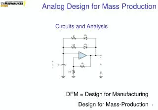
Circuits and Analysis
Circuits and Analysis. DFM = Design for Manufacturing Design for Mass-Production. eCAD Tools. Pspice Freeware Simulator (~6MB download) Includes simple schematic capture & analog simulator http://www.linear.com/designtools/softwareRegistration.jsp.

Circuits and Analysis
E N D
Presentation Transcript
Circuits and Analysis • DFM = Design for Manufacturing • Design for Mass-Production
eCAD Tools Pspice Freeware Simulator (~6MB download) Includes simple schematic capture & analog simulator http://www.linear.com/designtools/softwareRegistration.jsp Includes full suite of Cadence Tools for Academic Use ONLY! http://www.cse.ogi.edu/CFST/tut/help/pspice_examples.html
Current: Sum of the currents at any node must equal 0. Currents Entering = Currents Exiting Voltage:Sum of the voltages in a circuit loop must equal 0. Voltages Supplied = Voltages Dropped Recall the Basic Kirchhoff’s Circuit Laws
Capacitor Review • Static Characteristics: C = Q/V • Where 1 Farad = 1 Coulomb per 1 Volt • If C is constant and I try to store more charge on C, its voltage will increase proportionally • If C is constant and I want to increase the voltage across it, I need to add more charge • Dynamic Characteristics: I(t) = C dV/dt • where; I(t) = capacitor charging current (Amps) • dV/dt = capacitor voltage change (Volt/Sec) • Note: If I(t) is constant, V(t) is a ramping voltage • Laplace Impedance 1/sC • Complex Impedance 1/jwC • Capacitors Add Directly in Parallel Circuit: CEQ = C1 + C2 +…CN • Capacitors Add Inversely in Series Circuit: CEQ-1 = C1-1 + C2-1 +…CN-1
Dynamic RC Circuit Behavior Review + Where t = RC (time constant)
Inductor Review • Static Characteristics: L = Fm/I • Where 1 Henry = 1 Weber (Mag Flux) per Amp • Note: 1 Henry = 1 Volt per Amp/Sec = 1 Volt-Sec/Amp • Dynamic Characteristics: V(t) = L dI/dt • Where; V(t) = inductor voltage • dI/dt = inductor current change (Amp/Sec) • Note: If DC current thru an inductor is abruptly stopped (circuit opened), the induced voltage V(t) will “spike” very high • Laplace Impedance sL • Complex Impedance jwL • Inductors Add Directly in Series Circuit: LEQ = L1 + L2 +…LN • Inductors Add Inversely in Parallel Circuit: LEQ-1 = L1-1 + L2-1 +…LN-1
Dynamic RL Circuit Behavior Review V/R V Current Voltage
Parallel Resonance (Infinite Impedance) Parallel Impedance Z = sL // (sC)-1 Z = (sL)(sC)-1 / (sL + (sC)-1) Z = sL / (s2LC + 1) jwL / (-w2LC + 1) Note Z Infinity when w2 = LC w = (LC)-1/2 (f = 2pw ) Series Resonance (Zero Impedance) Series Impedance Z = sL + (sC)-1 Z = s2LC + 1 -w2LC + 1 Note Z 0 when w2 = LC w = (LC)-1/2
Electrolytic & Electric Double Layer • Rolled-Wet electrolyte construction • Very Polarized, Low Voltage Range • Ultra High Capacitance Density (5000F available) • High Cost • Used in Power Supplies, Power Backup Systems • Listed on WEEE Restrictions – Item # 15 (2.5x2.5cm) • Reliability Risk for High Temp or High Vibration Apps
Tantalum • Solid Dielectric construction • Polarized • Medium-High Capacitance Density • Low Voltage Range • Used for Board Large (Bulk) Decoupling • Rectangular SMT package • Ceramic • Solid Dielectric construction in single & multilayered • Non-polarized, High Voltage Range • Low Capacitance Density • Low Cost • Used for IC decoupling, low precision timing, filters • Rectangular SMT package
Polyester Film, Metalized Polyester Film • Solid Dielectric construction in multilayered • Non-polarized, High Voltage Range • Medium Cost • Low Capacitance Density • Used for medium precision timing, filters • Rectangular SMT packages • Polypropylene • Solid Dielectric construction • Non-polarized, High Voltage Range • Medium Cost, Low Capacitance Density • Very Low Leakage • Used for high precision timing, filters, sample-hold • Rectangular SMT packages
Inductors • Air Core , Ferrous Core Stick & Ferrous Core Toroid • Note: Air Core May Induce Large Stray Fields • Shielded and Unshielded • Inductance will Have Resistance • Thru Hole & SMT packages • Rated for Inductance, Max Current, Frequency
Passive Components, R-L-C • Critical Factors: • Ambient Temperature • Thermal Deratings & Variation of Primary Parameter (Temp Co) • Maximum Imposed Voltage and/or Current • Maximum Imposed dV/dT and/or Frequency • Inductive Frequency (high frequency model) • Minimum Analysis & Selection Considerations: • Primary Parameter Tolerances (R, L, C %) • Total Power vs Package Dissipation • Maximum Voltage • Composition, Specific die-electrics, construction, etc
Passive Discretes • Resistors/Inductors: Must specify or account for Tolerance, Power, Package and Temp Coefficient • Derating Guide: ~50% of rated power or current • Std Tolerances: 0.1%, 1%, 5%, 10% and 20% • Constructional Anomalies: Max Voltage, Inductive with High Freq • Capacitors: Must specify or account for Tolerance, WV, Polarization, Dielectric, Temp Co and Package • Derating Guide: ~50% of rated voltage • Std Tolerances: 1%, 2%, 5%, 10%, 20%, 80% • Constructional Anomalies: Charge Leakage, Inductive with High Freq,
+ - • Amplifiers
Simple Small Signal Models for the BJT Figure 4.33 Small-signal equivalent circuits for the BJT.
Common Emitter Amplifier & Small Signal Equivalent Circuit Voltage Gain: Av = vO/vIN = - bAC (RC//RL) (rp + (1 + bAC)RE1) Current Gain: Ai = iO/iIN = - bAC RC(R1//R2)/(RC+RL) (rp + (1 + bAC)RE1) + (R1//R2) Input Impedance: Ri = vIN/iIN = (R1//R2)//(rp + (1 + bAC)RE1)
Transistor Amplifier Load Line Analysis VCC/RDC VCC DC or Static Load Line:VCC = ICRC + VCEq + (IC + IB)RE Note IC = (bDC)IB & RE = RE1 + RE2 VCC = IC (RC + RE + RE/ bDC) + VCEq = IC (RDC) + VCEqwhere RDC = RC + RE + RE/ bDC Now put into the form Y = mX = b where Y = IC & X = VCE IC = VCE (-RDC )-1 + VCC (RDC )-1 Y intercept = VCC/RDC X intercept = VCC
Transistor Amplifier Load Line Analysis • AC or Dynamic Load Line: • VCC = ICq (RDC) + iCq (RAC) + vCE + VCEqwhere RAC = RC//RL + RE1 + RE1/ bAC • In the form Y = mX + b IC = VCE (-RAC )-1 + (VCEq/RAC + ICq ) • Y intercept = VCEq/RAC + ICq X intercept = VCC - ICq (RDC -RAC) The AC or Dynamic Load Line shows the slope the amplifier will actually operate on with signal swing
Transistor Amplifier Load Line Analysis Yd Ys Q Xd Xs Load Line Comparison: Static: IC = VCE (RDC )-1 + VCC (RDC )-1 Ys = VCC/RDC Xs = VCC Dynamic: IC = VCE (RAC )-1 + (VCEq/RAC + ICq ) Yd = VCEq/RAC + ICq Xd = VCC - ICq (RDC -RAC) Quiescent Point Q will be at Intersection, For Best Q Point - Bisect the AC Load Line End Points Note: For Capacitively Coupled Loads RAC < RDC Therefore Set ICq = VCC/(RDC + RAC)
General Linear Analog Circuits • Amplifiers and Attenuators • Math Functions (add, subtract) • Oscillators (sinusoidal) • Filters • Voltage Regulators • Voltage References
General Non-Linear Analog Circuits • Comparators • Oscillators (non-sinusoidal, square, sawtooth, etc) • Voltage Limiters and Clamps • Rectifiers and Bridges • Math Functions (multiply, divide) • Log and other Non-linear Amplifiers • Sample and Hold Amplifiers • Envelope & Peak Detectors • Phase Detectors • Phased Locked Loops • Switching Voltage Regulators
Small Signal Amplifiers • Critical Factors: • Component Tolerances, particularly gain setting R’s, Transistor B • OpAmp Input Offset Voltage (Vio), worse for high gain • Input Bias Current (Ib), Input Offset Current (Iio) • Finite Diff Gain (Ad) & Variation of Ad with Frequency • Output Slew Rate and Output Vp-p at Maximum Frequency • Typical DFM Analysis: • Total DC Offset error in Volts (1,2,3) • Total Gain Error vs Nominal, Converted to Volts (1,4) • Power Bandwidth for Application (1,5)
Basic Gain in Voltage, Current or CombinationLinear Operation: No New Frequencies Created! • Voltage Amplifiers (Vin >> Vout): Av = Vout/Vin • Current Amplifiers (Iin >> Iout): Ai = Iout/Iin • Transimpedance (Iin >> Vout): Zm = Vout/Iin • Transconductance (Vin >> Iout): Gm = Iout/Vin Additional Parameters • Input Impedance: Zin = Vin/Iin • Output Impedance: Zout = {Vout(NL) – Vout(L)}/Iout • Slew Rate (SR): Min dVout/dT • Slew Rate BW = SR/2pVp where Vp = Peak Voltage
+ - Operational Amplifier – Why?Linear, Differential, High Gain Amplifier Advantages Over Single Ended Amplifier Block ?? • Easy to add positive and negative feedback with differential input • Single Ended Application Gains can be tightly controlled with external components and made insensitive to internal transistor gain variations • Inherent noise rejection when noise enters both input terminals
+ - Operational AmplifierIdeal Assumptions Vp Used for basic analysis, nominal gain analysis Vout • Vout = Ad (Vp – Vn) where Ad is the diff gain • Ad = Infinite • Zin = Infinite, Iin = 0 where Iin is the input current • Vp = Vn because of infinite Ad, Vo may be non-zero under this condition • Iout = Infinite (Often a false assumption) These basic assumptions allow simple circuit analysis to determine Nominal gain applications Vn
+ - Operational AmplifierPower Supplies Vcc Vp Power Supplies can be a critical consideration Vout • -Vcc < Vout < Vcc At all times, Vout(max) may be as low as 2 to 5 volts below Vcc depending upon model • Vcc, -Vcc sometimes referred to as “Rails” due to power distribution on some boards resembling tracks • Many applications use “Split” supply Operation • Split Supply means Vcc = |-Vcc| • Some models characterized for 1 supply operation (but ALL will work there) • Single Supply means –Vcc = 0 • Vcc, -Vcc power pins should always be capacitively filtered with 0.1uf (usually ceramic monolithic X7R or similar) Vn -Vcc
Operational AmplifierMany Types Available • Others: • Video • Current Feedback • Power • Chopper Stabilized • Electrometer
+ - Operational AmplifierBasic Applications Rf Av = - Rf/Ri Zin = Ri Inverting Voltage Amp Ri Vin Vout Rp
+ - Operational AmplifierBasic Applications Ri Av = 1 + Rf/Rp Zin = Ri + Non-Inverting Voltage Amp When Rf=0, Rp=~Infinite…… Av = 1 Vin Vout Rf Rp 8
+ - Operational AmplifierBasic Applications Av = 1 Zin = Unity Gain Voltage Amp Vin Vout 8
+ - Operational AmplifierBasic Applications Ri Gm = 1/Rp Zin = Ri + Transconductance Amp Vin RL Iout Rp 8
+ - Operational AmplifierBasic Applications Rf Zm = - Rf Transimpedance Amp Iin Vout RL
+ - Operational AmplifierBasic Applications Ai = -(1 + Ri/Rp) Current Amplifier Iin RL Ri Iout Rp
+ - Operational AmplifierIdeal Assumptions Vp Used for basic analysis, nominal gain analysis Vout • Vout = Ad (Vp – Vn) where Ad is the diff gain • Ad = Infinite • Zin = Infinite, Iin = 0 where Iin is the input current • Vp = Vn because of infinite Ad, Vo may be non-zero under this condition • Iout = Infinite (Often a false assumption) These basic assumptions allow simple circuit analysis to determine Nominal gain applications Vn
+ - Operational AmplifierReal Characteristics Ip Vp Vout Used for more accurate Gain Characterization Iout Vio • Vout = Ad(Vp – Vn) + Ac(Vp + Vn)/2 + Vio Ad is the diff gain, Ac is the common mode gain, Vio = offset voltage • CMRR = Common Mode Rejection Ratio = 20log(Ad/Ac) • Ib = Bias Current (Ave Current = [Ip + In]/2) • Iio = Offset Current (Diff Current = Ip – In) • Iout = Finite, Split between gain set components and load • Vio = Input Diff Voltage reflected back from Vo under the condition the Vp = Vn = 0 Use superposition to understand contributions In Vn
+ - Operational AmplifierReal Characteristic Effects Basic Strategy Vp • Consider the Effect Separately, then combine results • Show Ib and Iio as input current sources • Show Vio as diff voltage on Vp-Vn • Use amended opamp in std application circuit, Vin=0 (grounded). • Find Vout, all Vout will be Verror due to Offset and Bias Vout Vn
+ - Inverting ConfigurationOffset Error Contribution 1 Rf Ii = (0-Vio)/Ri If = (Vio-Vo)/Rf Ii = If Vo = Vio(1 + Rf/Ri) = Verr Inverting Voltage Amp Error Voltage due to Vio Ri If Vout Vio Ii Rp
+ - Non-inverting ConfigurationOffset Error Contribution 1 Ri Ii = (0-Vio)/Rp If = (Vio-Vo)/Rf Ii = If Vo = Vio(1 + Rf/Rp) = Verr Non-Inverting Voltage Amp Error Voltage due to Vio Vin Vout Vio Rf If Rp Ii
+ - Inverting AmplifierOffset Error Contribution 2 Rf At V+: Iio = Ib + V+/Rp V+ = Rp(Iio-Ib) At V-: -V-/Ri = (V--Vout)/Rf + Ib + Iio Sub V+ into above equation Vo = Verr = Rf(Ib-/+Iio) - [((RfRp)/Ri + Rp)(Ib+/-Iio)] Note if Iio = ~0 and Rp = Rf//Ri, then Verr = 0 Verr is always minimized when Rp = ~Rf//Ri Inverting Voltage Amp Error Voltage due to Ib, Iio Ri If Vin Vout Iio Ii Ib Ib Rp
+ - Non-Inverting AmplifierOffset Error Contribution 2 Rf At V+: Iio = Ib + V+/Ri V+ = Ri(Iio-Ib) At V-: -V-/Rp = (V--Vout)Rf + Ib + Iio Sub V+ into above equation Vo = Verr = Rf(Ib-/+Iio) - [((RfRi)/Rp + Ri)(Ib+/-Iio)] Note if Iio = ~0 and Ri = Rf//Rp, then Verr = 0 Verr is always minimized when Ri = Rf//Rp Non-Inverting Voltage Amp Error Voltage due to Ib, Iio Rp If Vout Iio Ip Ib Ib Ri Ii Vin
+ - Inverting AmplifierGain Error Rf Av (nom) = - Rf/Ri But Assume Vout = Ad(V+ - V-) Find expressions for V+ & V- Substitute into above Vout Solve for Vout/Vin = Av Av = -(RfAd)/(RiAd + Ri + Rf) Av = Av(nom)/CF CF = Correction Factor CF = 1 + 1/Ad + Rf/(RiAd) |Av| < |Av (nom)| Inverting Voltage Amp Ri If Vin Vout Ii Rp Don’t Forget to Factor in Res Tol% !