Download

1 / 91
920 likes | 1.15k Vues
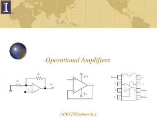
Operational Amplifiers. 1. Figure 2.1 Circuit symbol for the op amp. Figure 2.2 The op amp shown connected to dc power supplies. Figure 2.3 Equivalent circuit of the ideal op amp.

E N D
Figure 2.1 Circuit symbol for the op amp. Microelectronic Circuits - Fifth Edition Sedra/Smith
Figure 2.2 The op amp shown connected to dc power supplies. Microelectronic Circuits - Fifth Edition Sedra/Smith
Figure 2.3 Equivalent circuit of the ideal op amp. Microelectronic Circuits - Fifth Edition Sedra/Smith
Figure 2.4 Representation of the signal sources v1 and v2 in terms of their differential and common-mode components. Microelectronic Circuits - Fifth Edition Sedra/Smith
Figure E2.3 Microelectronic Circuits - Fifth Edition Sedra/Smith
Figure 2.5 The inverting closed-loop configuration. Microelectronic Circuits - Fifth Edition Sedra/Smith
Figure 2.6 Analysis of the inverting configuration. The circled numbers indicate the order of the analysis steps. Microelectronic Circuits - Fifth Edition Sedra/Smith
Figure 2.7 Analysis of the inverting configuration taking into account the finite open-loop gain of the op amp. Microelectronic Circuits - Fifth Edition Sedra/Smith
Figure 2.8 Circuit for Example 2.2. The circled numbers indicate the sequence of the steps in the analysis. Microelectronic Circuits - Fifth Edition Sedra/Smith
Figure 2.9 A current amplifier based on the circuit of Fig. 2.8. The amplifier delivers its output current to R4. It has a current gain of (1 + R2/R3), a zero input resistance, and an infinite output resistance. The load (R4), however, must be floating (i.e., neither of its two terminals can be connected to ground). Microelectronic Circuits - Fifth Edition Sedra/Smith
Figure E2.5 Microelectronic Circuits - Fifth Edition Sedra/Smith
Figure E2.6 Microelectronic Circuits - Fifth Edition Sedra/Smith
Figure 2.10 A weighted summer. Microelectronic Circuits - Fifth Edition Sedra/Smith
Figure 2.11 A weighted summer capable of implementing summing coefficients of both signs. Microelectronic Circuits - Fifth Edition Sedra/Smith
Figure 2.12 The noninverting configuration. Microelectronic Circuits - Fifth Edition Sedra/Smith
Figure 2.13 Analysis of the noninverting circuit. The sequence of the steps in the analysis is indicated by the circled numbers. Microelectronic Circuits - Fifth Edition Sedra/Smith
Figure 2.14 (a) The unity-gain buffer or follower amplifier. (b) Its equivalent circuit model. Microelectronic Circuits - Fifth Edition Sedra/Smith
Figure E2.9 Microelectronic Circuits - Fifth Edition Sedra/Smith
Figure E2.13 Microelectronic Circuits - Fifth Edition Sedra/Smith
Figure 2.15 Representing the input signals to a differential amplifier in terms of their differential and common-mode components. Microelectronic Circuits - Fifth Edition Sedra/Smith
Figure 2.16 A difference amplifier. Microelectronic Circuits - Fifth Edition Sedra/Smith
Figure 2.17 Application of superposition to the analysis of the circuit of Fig. 2.16. Microelectronic Circuits - Fifth Edition Sedra/Smith
Figure 2.18 Analysis of the difference amplifier to determine its common-mode gain Acm;vO/ vIcm. Microelectronic Circuits - Fifth Edition Sedra/Smith
Figure 2.19 Finding the input resistance of the difference amplifier for the case R3 = R1 and R4 = R2. Microelectronic Circuits - Fifth Edition Sedra/Smith
Figure 2.20 A popular circuit for an instrumentation amplifier: (a) Initial approach to the circuit; (b) The circuit in (a) with the connection between node X and ground removed and the two resistors R1 and R1 lumped together. This simple wiring change dramatically improves performance; (c) Analysis of the circuit in‘ (b) assuming ideal op amps. Microelectronic Circuits - Fifth Edition Sedra/Smith
Figure 2.21 To make the gain of the circuit in Fig. 2.20(b) variable, 2R1 is implemented as the series combination of a fixed resistor R1f and a variable resistor R1v. Resistor R1f ensures that the maximum available gain is limited. Microelectronic Circuits - Fifth Edition Sedra/Smith
Figure 2.22 Open-loop gain of a typical general-purpose internally compensated op amp. Microelectronic Circuits - Fifth Edition Sedra/Smith
Figure 2.23 Frequency response of an amplifier with a nominal gain of +10 V/V. Microelectronic Circuits - Fifth Edition Sedra/Smith
Figure 2.24 Frequency response of an amplifier with a nominal gain of –10 V/V. Microelectronic Circuits - Fifth Edition Sedra/Smith
Figure 2.25 (a) A noninverting amplifier with a nominal gain of 10 V/V designed using an op amp that saturates at ±13-V output voltage and has ±20-mA output current limits. (b) When the input sine wave has a peak of 1.5 V, the output is clipped off at ±13 V. Microelectronic Circuits - Fifth Edition Sedra/Smith
Figure 2.26 (a) Unity-gain follower. (b) Input step waveform. (c) Linearly rising output waveform obtained when the amplifier is slew-rate limited. (d) Exponentially rising output waveform obtained when V is sufficiently small so that the initial slope (vtV) is smaller than or equal to SR. Microelectronic Circuits - Fifth Edition Sedra/Smith
Figure 2.27 Effect of slew-rate limiting on output sinusoidal waveforms. Microelectronic Circuits - Fifth Edition Sedra/Smith
Figure 2.28 Circuit model for an op amp with input offset voltage VOS. Microelectronic Circuits - Fifth Edition Sedra/Smith
Figure E2.23 Transfer characteristic of an op amp with VOS = 5 mV. Microelectronic Circuits - Fifth Edition Sedra/Smith
Figure 2.29 Evaluating the output dc offset voltage due to VOS in a closed-loop amplifier. Microelectronic Circuits - Fifth Edition Sedra/Smith
Figure 2.30 The output dc offset voltage of an op amp can be trimmed to zero by connecting a potentiometer to the two offset-nulling terminals. The wiper of the potentiometer is connected to the negative supply of the op amp. Microelectronic Circuits - Fifth Edition Sedra/Smith
Figure 2.31 (a) A capacitively coupled inverting amplifier, and (b) the equivalent circuit for determining its dc output offset voltage VO. Microelectronic Circuits - Fifth Edition Sedra/Smith
Figure 2.32 The op-amp input bias currents represented by two current sources IB1 and IB2. Microelectronic Circuits - Fifth Edition Sedra/Smith
Figure 2.33 Analysis of the closed-loop amplifier, taking into account the input bias currents. Microelectronic Circuits - Fifth Edition Sedra/Smith
Figure 2.34 Reducing the effect of the input bias currents by introducing a resistor R3. Microelectronic Circuits - Fifth Edition Sedra/Smith
Figure 2.35 In an ac-coupled amplifier the dc resistance seen by the inverting terminal is R2; hence R3 is chosen equal to R2. Microelectronic Circuits - Fifth Edition Sedra/Smith
Figure 2.36 Illustrating the need for a continuous dc path for each of the op-amp input terminals. Specifically, note that the amplifier will not work without resistor R3. Microelectronic Circuits - Fifth Edition Sedra/Smith
Figure 2.37 The inverting configuration with general impedances in the feedback and the feed-in paths. Microelectronic Circuits - Fifth Edition Sedra/Smith
Figure 2.38 Circuit for Example 2.6. Microelectronic Circuits - Fifth Edition Sedra/Smith
Figure 2.39 (a) The Miller or inverting integrator. (b) Frequency response of the integrator. Microelectronic Circuits - Fifth Edition Sedra/Smith
Figure 2.40 Determining the effect of the op-amp input offset voltage VOS on the Miller integrator circuit. Note that since the output rises with time, the op amp eventually saturates. Microelectronic Circuits - Fifth Edition Sedra/Smith
Figure 2.41 Effect of the op-amp input bias and offset currents on the performance of the Miller integrator circuit. Microelectronic Circuits - Fifth Edition Sedra/Smith
Figure 2.42 The Miller integrator with a large resistance RF connected in parallel with C in order to provide negative feedback and hence finite gain at dc. Microelectronic Circuits - Fifth Edition Sedra/Smith
Figure 2.43 Waveforms for Example 2.7: (a) Input pulse. (b) Output linear ramp of ideal integrator with time constant of 0.1 ms. (c) Output exponential ramp with resistor RF connected across integrator capacitor. Microelectronic Circuits - Fifth Edition Sedra/Smith