Download
1 / 7
70 likes | 94 Vues
In This Paper, The Variable Input Voltage And Fixed Output Voltage DC To DC Converter For Photovoltaic System PV System Is Designed, Simulated And Constructed. There Are Three Main Portions In The Proposed System. They Are Solar Power Sensing System, The Controlling System And DC To DC Converter. In The Solar Power Sensing System, NPN Transistors 2SC 945 Are Used For Voltage Sensor And Logic Converter. In The Controlling System, PIC 16F876A Is Used To Determine The Solar Power Level And Control The DC To DC Converter. It Also Reads The Input And Output Voltage Values Of The DC To DC Converter Using Its Analog To Digital Converter A D Converter And Shows This Value On The Four Seven Segments Light Emitting Diodes Leds . The Developed Program For PIC 16F876A Is Tested With Proteus Simulation Software. In The DC To DC Converter, TL 494 Switch mode Pulse Width Modulation Control Circuit Is Used To Control The Power MOSFET Which Drives The Ferrite Core Transformer High Frequency Transformer Or Power Transformer . Dr. Thida Aung "Fixed Output DC to DC Converter for Photovoltaic System" Published in International Journal of Trend in Scientific Research and Development (ijtsrd), ISSN: 2456-6470, Volume-3 | Issue-5 , August 2019, URL: https://www.ijtsrd.com/papers/ijtsrd27988.pdf Paper URL: https://www.ijtsrd.com/engineering/electronics-and-communication-engineering/27988/fixed-output-dc-to-dc-converter-for-photovoltaic-system/dr-thida-aung<br>

E N D
International Journal of Trend in Scientific Research and Development (IJTSRD) Volume 3 Issue 5, August 2019 Available Online: www.ijtsrd.com e-ISSN: 2456 – 6470 Fixed Output DC to DC Converter for Photovoltaic System Dr. Thida Aung Professor and Head, Electronic Engineering Department, Technological University, Lashio, Northern Shan State, Myanmar How to cite this paper: Dr. Thida Aung "Fixed Output DC to DC Converter for Photovoltaic System" International Journal of Trend in Scientific Research and Development (ijtsrd), ISSN: 2456- 6470, Volume-3 | Issue-5, August 2019, pp.2137-2143, https://doi.org/10.31142/ijtsrd27988 Copyright © 2019 by author(s) and International Journal of Trend in Scientific Research and Development Journal. This is an Open Access article distributed under the terms of the Creative Commons Attribution License (CC (http://creativecommons.org/licenses/by /4.0) INTRODUCTION Solar Photovoltaic (PV) system is a renewable energy system and can provide safe, reliable, maintenance-free and environmental friendly source of power for a very long time. Millions of systems have been installed worldwide, in sizes ranging from a fraction of a watt to multi-megawatts. For many applications, solar electric systems are not only cost- effective but also least expensive option to produce the electrical power. In this paper, DC to DC converter cooperates with the solar modules to reduce the losses between the solar modules and the electrical load. By using the DC to DC converter in the solar system, the overall efficiencies of the system can be improved and the overall cost for the whole system can be reduced because DC to DC converter is the most suitable voltage regulating system. DC to DC converter is the advance form of the voltage regulator. In linear voltage regulator (series regulator), the input voltage must be higher than the output voltage. But the input voltage is not a major problem in the DC to DC converter. DC to DC converter can step-up, step-down and invert the input voltage. DC to DC converter has many other advantages than the linear voltage regulator. DC to DC converter stores the input power at the voltage or current storage devices such as inductor and capacitor. And then release this power to the electrical load with a switching process. Pulse Width Modulator (PWM) is the major component of the DC to DC converter. It produces the square wave pulse trains ABSTRACT In This Paper, The Variable Input Voltage And Fixed Output Voltage DC To DC Converter For Photovoltaic System (PV System) Is Designed, Simulated And Constructed. There Are Three Main Portions In The Proposed System. They Are Solar Power Sensing System, The Controlling System And DC To DC Converter. In The Solar Power Sensing System, NPN Transistors (2SC 945) Are Used For Voltage Sensor And Logic Converter. In The Controlling System, PIC 16F876A Is Used To Determine The Solar Power Level And Control The DC To DC Converter. It Also Reads The Input And Output Voltage Values Of The DC To DC Converter Using Its Analog To Digital Converter (A/D Converter) And Shows This Value On The Four Seven Segments Light Emitting Diodes (Leds). The Developed Program For PIC 16F876A Is Tested With Proteus Simulation Software. In The DC To DC Converter, TL 494 (Switch mode Pulse Width Modulation Control Circuit) Is Used To Control The Power MOSFET Which Drives The Ferrite Core Transformer (High Frequency Transformer Or Power Transformer). Keywords: DC to DC converter; photovoltaic system; PIC 16F876A; analog to digital converter; Published in IJTSRD27988 BY 4.0) and the pulse width of these pulse trains can be controlled with the external input track called feed-back track. The circuit components and designing of the DC to DC converter are more complex than traditional voltage regulator because of containing Pulse Width Modulator (PWM). But according to the development of the electronic techniques, PWM module can be achieved in the form of integrated circuits (ICs) or chip types in now. Many types of converter are widely used as mobile phone charger, DVD/VCD player power supply, TV power supply, PC power supply, laptop computer charger and many others electrical or electronic application. In the traditional photovoltaic system, photovoltaic modules are used to convert light energy into electricity. This electricity cannot be directly connected with the electrical load because the output voltage of the photovoltaic modules is the unregulated DC and varies 0 to +21V. The overall block diagram of the photovoltaic system is shown in Figure 1. The traditional photovoltaic system consists of six major modules; PV module, Solar charge controller, Inverter, Battery, Load and Auxiliary energy sources. Solar charge controller is used to control the charging voltage to the battery. The battery is used to storage power for further usage. Auxiliary energy source is used to charge the battery when the electrical power cannot be available from the solar modules (e.g., at night). The inverter is used to convert the DC power to the AC power if the system needs to produce AC power. @ IJTSRD | Unique Paper ID – IJTSRD27988 | Volume – 3 | Issue – 5 | July - August 2019 Page 2137
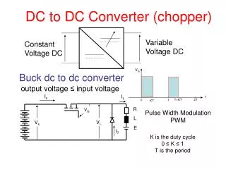
International Journal of Trend in Scientific Research and Development (IJTSRD) @ www.ijtsrd.com eISSN: 2456-6470 A DC to DC converter can be distinguished according to their converting properties. There are four types of DC to DC converter. They are Step-down converter (Buck converter), Step-up converter (Boost converter), Inverting converter and Transformer flyback converter. A.Step-down Converter (Buck Converter) In the buck converter, the output voltage of the converter is less than the input voltage. The required switching signal is provided by the pulse width modulator. The levels of the output voltage can be controlled by the pulse width of the switching signal. The frequency of the switching signal must be one of the fix frequency values ranging from 30 kHz to 300 kHz. The output voltage (Vo) is equal to the product of the duty cycle of the pulse (D) and the supply voltage (Vs). The basic sample circuit diagram of the buck converter is shown in Figure 3. Vo = D x Vs Where, VO = the output voltage of the converter (V) D = the duly cycle of the switching signal (%) Vs = the supply voltage to the converter (V) Figure 1 Block Diagram of the Photovoltaic System In this research work, DC to DC converter is used instead of solar charge controller and battery. Solar charge controller cannot regulate the input voltage coming from photovoltaic module. DC to DC converter can regulate the input voltage coming from photovoltaic module and it has many other advantageous than the solar charge controller. The output of the DC to DC converter can be used in many other electrical applications such as charging battery to be storage power for further use or directly using solar power during the light falling onto the PV panels. Implemented block diagram of the DC to DC converter for photovoltaic system is shown in Figure 2. In this system, the output of the DC to DC converter can be directly connected with the electrical load. The AC powercan be produced by connecting the output of the DC to DC converter with the inverter. PIC microcontroller is used to digitalize the system and to show the input and output voltages of the DC to DC converter. Equation 1 Figure3. The Basic Sample Circuit Diagram of the Buck Converter B.Step-up Converter (Boost Converter) In the boost converter, the output voltage of the converter is more than the input voltage. But the output current is less than the input current because the input and the output power are almost equal. The basic sample circuit diagram of the boost converter is shown in Figure 4. Figure 2 Implemented Block Diagram of the DC to DC Converter for Photovoltaic System Figure4. Basic Sample Circuit Diagram of the Boost Converter V V Where, VO = the output voltage of the converter (V) D = the duly cycle of the switching signal (%) Vs = the supply voltage to the converter (V) C.Inverting Converter The inverting converter can convert the input voltage. The output voltage can be more or less than the input voltage. The basic sample circuit diagram of the inverting converter is shown in Figure 5. II A DC to DC converter is one of the switching regulator types. It uses the switching process to transfer the power from the source to the load. It stores the input power at the voltage or current storage devices such as capacitor or inductor. And then release this power to the electrical load with a switching process. Pulse Width Modulator (PWM) is determined the on or off periods of the switch. PWM is the major component of the DC to DC converter. It produces the on/off signaling pulse train. This signaling pulse train is used to control the switch. The frequency of the pulse train is range from 30 kHz to 300 kHz according to the design of the converter. LITERATURE REVIEW o s (1 - D) Equation 2 @ IJTSRD | Unique Paper ID – IJTSRD27988 | Volume – 3 | Issue – 5 | July - August 2019 Page 2138
International Journal of Trend in Scientific Research and Development (IJTSRD) @ www.ijtsrd.com eISSN: 2456-6470 Where, VO = the output voltage of the converter (V) D = the duly cycle of the switching signal (%) Vs = the supply voltage to the converter (V) N1 = the number of primary winding of the Transformer (turns) N2 = the number of secondary winding of the Transformer (turns) III SOFTWARE IMPLEMENTATION A.Operation of the DC to DC Converter for PV System Figure 5 Basic Sample Circuit Diagram of the Inverting Converter D x V s o V (1 - D) Equation 3 The main flowchart of the DC to DC converter for PV system is illustrated in Figure 7. There are four main units. They are solar panel, solar power sensor, PIC microcontroller and DC to DC converter. The solar panel converts the sunlight into electricity. This electricity is the form of direct current (DC) with the voltage range of 0 to 21V. The coming voltages from the solar panel are measured by the solar power sensor. If the voltage is less than +8V, it produces logic ‘0’ (0V) to the PIC. If the voltage is more than +8V, it produces logic ‘1’ (+5V). The PIC is act as the Central Processing Unit (CPU). It checks the output of the solar power sensor. When the solar power sensor’s output is low (logic ‘0’), it turns on the solar power low indicator. When the solar power sensor’s output is high (logic ‘1’), it turns on the DC to DC converter. After the DC to DC converter turns on, PIC reads the input voltage of the converter and displays this voltage value on the input voltages LED display and then reads the output voltage of the converter and displays this voltage values on the output voltages LED display. Where, VO = the output voltage of the converter (V) D = the duly cycle of the switching signal (%) Vs = the supply voltage to the converter (V) D.Transformer Flyback Converter Transformer flyback converter is the advance form of the buck, boost and inverting converters. This type of converter is used in this research work because it is the efficient form of all of the converter types and the converter used in the system is needed to step-up and step-down the input voltage. This requirement can be solved only by the use of transformer flyback type DC to DC converter. All of the transformer flyback converter can be achieved electrical isolation and non-isolation types. In electrical isolation type, the output side and the input side have no electrical connection between them. The basic sample circuit diagram of transformer flyback converter is shown in Figure 6. There are two types of transformer flyback converter. They are single-output type and the multi-output type. In single-output type, the output voltage can be obtained by stepping-up, stepping-down the input voltage. In multi-output type, the output voltage can be obtained by stepping-up, stepping- down and inverting the input voltage at the same time. (a) (b) Figure 6 The Basic Sample Circuit Diagram of the Transformer Flyback Converter, (a) Single-output Type, (b) Multi-output Type The output voltage of the converter can be calculated by the Equation 4. N x D) - (1 D Figure 7 Main Flowchart of the System V 1 V x o s N Equation 4 2 @ IJTSRD | Unique Paper ID – IJTSRD27988 | Volume – 3 | Issue – 5 | July - August 2019 Page 2139
International Journal of Trend in Scientific Research and Development (IJTSRD) @ www.ijtsrd.com eISSN: 2456-6470 B.PIC Control System This flowchart shown in Figure 8 is represented for the whole controlling, calculation and processing for the system. As the first step, the PIC is configured its ports or pins as the digital or analog, input or output pins. After the pins are assigned, determine the solar power level by checking the solar power sensor output, weather active (logic high) or inactive (logic low). If the solar power sensor output is inactive (logic low), the PIC will send out the logic high signal to the solar power low indicator and then check the solar power sensor again and serves this sequence until the solar power sensor output is active (logic high). If the solar power sensor output is active (logic high), the PIC will send out the logic high signal to the DC to DC converter to turn on the converter. After the converter is turned on, the PIC reads the input voltages of the DC to DC converter by using it’s analog to digital converter module and shows the relative voltages on the input voltages display and then the PIC reads the converter output voltages and shows the relative voltages on the output voltages display. The flowchart of the PIC to control the DC to DC converter for the PV system is shown in Figure 8. Figure 9 the Flowchart for Flashing Solar Power Low Indicator If the RC4 is low, the PIC gives out the high signal to the RC5 and maintains this signal for 500ms and then the PIC is clear this high signal of the RC5 and maintains this clear signal (logic low) for 500 ms and checks the solar power sensor again. The PIC operates this sequence until the solar power sensor’s output is high. IV HARDWARE IMPLEMENTATION The circuit of the DC to DC converter for PV system contains two main modules. The first module is the controlling module. Controlling module contains the functions of determining the level of solar power, controlling the DC to DC converter and displaying input and output voltages of the converter on the LED display. All of the controlling and execution functions of the controlling module are done by the use of PIC 16F876A. The second module is the DC to DC converter module. This module contains pulse width modulator (PWM) section using TL 494 (pulse width modulation control circuit), power switch section using IRF Z44N (power MOSFET) and the feedback section using resistor network. A.Circuit Design for Solar Power Sensor Solar power sensor is the important module for the central controlling module because operating or non-operating conditions of the whole system depends on its output. The Solar power sensor used in this system is expressed in Figure 10. Figure 8 the Flowchart of PIC Control System of the DC to DC Converter for PV System C.Flashing Solar Power Indicator When the solar power is low, the PIC turns on the solar power low indicator. In this stage, the solar power low indicator is designed to flash with the time period of 500 milli-seconds. The flowchart for flashing solar power low indicator is shown in Figure 9. Figure 10 Circuit Diagram of the Solar Power Sensor @ IJTSRD | Unique Paper ID – IJTSRD27988 | Volume – 3 | Issue – 5 | July - August 2019 Page 2140
International Journal of Trend in Scientific Research and Development (IJTSRD) @ www.ijtsrd.com eISSN: 2456-6470 The Solar power sensor contains two main parts. One is the voltage sensor and the second is the logic converter. The voltage sensor is the under voltage lock-out circuit. Only one NPN transistor is used in this section. The logic converter is the inverting amplifier. All of the transistors are used as switch types. The voltage drop at the base of the transistor Q1 is equal to the voltage drop across the variable resistor R2. The voltage drop across the variable resistor R2 can be calculated by the Equation 5. R V 2 Where, VR2 = Voltage drop across the variable resistor R2 (V) R1 = Resistance of the resistor R1 (Ω) R2 = Resistance of the resistor R2 (Ω) VCC = Supply voltage (V) B.Circuit Design for PWM Module TL 494 pulse width modulation control circuit is used to produce the required switching signal for the power MOSFET. The circuit diagram is expressed in Figure 11. Pin 4 of the TL 494 is used to control (on or off) the whole converter. When the logic state of this pin is low, the pulse width modulation module within the TL 494 operates and produces the switching signal to the switching circuit from pins 9 and 10 of the TL 494. If the logic state of pin 4 is high, the pulse width modulation module within the TL 494 does not operate. The transistor Q3, zener diode D7 and resistors R18 and R19 are act as the logic inverter circuit. If the PWM control signal is high (logic '1'), the collector voltage of the Q3 is approach to zero and the PWM control signal is low (logic '0'), the collector voltage of the Q3 is almost equal to +5V. The feedback input track is the analog pin and the amount of voltages can control the duty cycle of the output frequency produced by the PWM module. Where, fout = The output frequency of the TL 494 (Hz) RT = Timing resistor () CT = Timing capacitor (F) C.Circuit Design for Switching Circuit 2 xV R CC R R Equation 5 1 2 Figure 12 Switching Circuit The main function of the switching circuit is to control the power transformer and to amplify the switching signal. The circuit diagram is sketched in Figure 12. Resistor R16 and R17 are act as the voltage divider network to drop the some amount of voltage from the PWM module and prevent the power MOSFET from damaging by the exceed of gate voltage. D5 is act as the AC filtering circuit. If the output signal of the PWM module has an AC component, the diode D5 will filter out this AC component signal. Assuming the power losses due to the output transformer and MOSFET as 10% and thus the efficiency of the whole converter circuit will be 90%. D.Circuit Design for Power Transformer The power transformer is used to transfer the electrical power from the primary side to the secondary side. The schematic diagram for the power transformer and rectifier circuit is demonstrated in Figure 13. The diode D4 and capacitor C6 are act as a rectifier circuit. The D4 is used to extract the positive half-cycle of the AC signal flowing out from the power transformer and the capacitor C6 is used to smooth the output DC. Figure 13 Power Transformers and Rectifier Circuit The output voltages of the power transformer and rectifier circuit can be calculated by the following equation; N x D 1 Where, VO = the output voltages of the power transformer and rectifier circuit (V) Vs = the supply voltages of the circuit (V) D = Duty cycle of the transformer (%) N1 = the number of primary winding of the Transformer (turns) N2 = the number of secondary winding of the Transformer (turns) Figure 11 Circuit Diagram of the Pulse Width Modulation Control D P V V x O S N The output frequency of the TL 494 used in this thesis is almost 5 kHz. The resistance value of the resistor RT is 35k and the capacitance value of the CT is 1nF. The output frequency of the pulse width modulation control circuit can be derived by the Equation 6. 1.1 f Equation 6 Equation 7 S out ( R x C ) T T @ IJTSRD | Unique Paper ID – IJTSRD27988 | Volume – 3 | Issue – 5 | July - August 2019 Page 2141
International Journal of Trend in Scientific Research and Development (IJTSRD) International Journal of Trend in Scientific Research and Development (IJTSRD) @ www.ijtsrd.com www.ijtsrd.com eISSN: 2456-6470 V. The simulation diagram of the central controlling unit using PIC16F876A for the DC to DC converter for PV system is demonstrated in Figures 14 and 15. Operating diagram (solar power high condition) is shown in Figure 14 and non operating diagram (solar power low condition) is shown in Figure 15. SIMULATION OF THE OVERALL SYSTEM SIMULATION OF THE OVERALL SYSTEM The simulation diagram of the central controlling unit using 6A for the DC to DC converter for PV system is demonstrated in Figures 14 and 15. Operating diagram (solar power high condition) is shown in Figure 14 and non- operating diagram (solar power low condition) is shown in When the input voltage is between 12 to 25V, the converter operates in step-down converting mode. The maximum input voltage should not exceed more than +25V. The photograph of the DC to DC converter running in step illustrated in Figure 17. When the input voltage is between 12 to 25V, the converter down converting mode. The maximum input voltage should not exceed more than +25V. The photograph of the DC to DC converter running in step-up mode is Figure 14 Simulation Diagram for Solar Power High Condition ram for Solar Power High Figure 17 DC to DC Converters Converters in Step-down Converting Mode Mode VII. The main circuit is designed with the three terminals positive voltage regulator (LM 7805), solar power sensor circuit (using transistors), programmable interface pulse width modulator (using TL 494), high frequency transformer (ferrite core transformer) and other electronic components (FET, resistor , capacitor and so on). LM 7805 is used to power the required supply voltage +5V DC of the PIC. Solar power sensor circuit is the simple sensor circuit and uses only two transistors. One is used to sense the voltage and the other is used as the logic converter in order to communicate with the PIC. PIC is used to check the output of the solar power sensor circuit, control the pulse width modulator or the whole system (e.g., operate or not) and calculation for A/D conversion is needed to display the input and output voltages of the converter. TL494 is the pulse width modulation control circuit used to sup switching signal of the switching circuit. Ferrite core transformer is used to transfer the source power to the load and to store the certain amount of power. FET is used to amplify the switching signal and to drive the transformer. Other electronic components are used as the need of the circuit design. By using the PIC in the DC to DC converter, the circuit is more efficient, reliable, powerful and effective. But it has a few drawbacks, such as high cost and can cause radio interference on the other devices (radio, television, etc.) VIII. FURTHER EXTENSION To reduce the total installation cost of the DC to DC converter, the pulse width modulator section (using TL 494) can be removed from the circuit because the microcontroller (PIC 16F876A) has the PWM module. Therefore, the required switching signal for the switching circuit can be provided by the PIC 16F876A. The DC to DC converter for PV system design and construction in this thesis can operate only in the day time because it has no storage devices to store the electric power. If the user wants to use this converter when the light is gone, the storage devices must be inserted in the system. the storage devices must be inserted in the system. CONCLUSION The main circuit is designed with the three terminals positive voltage regulator (LM 7805), solar power sensor circuit (using transistors), programmable interface controller (PIC), pulse width modulator (using TL 494), high frequency transformer (ferrite core transformer) and other electronic components (FET, resistor , capacitor and so on). LM 7805 is used to power the required supply voltage +5V DC of the PIC. lar power sensor circuit is the simple sensor circuit and uses only two transistors. One is used to sense the voltage and the other is used as the logic converter in order to communicate with the PIC. PIC is used to check the output of or circuit, control the pulse width modulator or the whole system (e.g., operate or not) and calculation for A/D conversion is needed to display the input and output voltages of the converter. TL494 is the pulse width modulation control circuit used to supply the required switching signal of the switching circuit. Ferrite core transformer is used to transfer the source power to the load and to store the certain amount of power. FET is used to amplify the switching signal and to drive the transformer. electronic components are used as the need of the Figure 15 Simulation Diagram for Solar Power Low Condition Figure 15 Simulation Diagram for Solar Power Low In Figure 14, As soon as the solar power sensor output is high (RC4 is high) the PIC 16F876A turns on the converter (RC6 is high), reads analog voltages and displays these voltages. In Figure 15, when the solar power is low (RC4 is low), the PIC 16F876A turns off the converter (RC6 is low) and turns on the solar power low indicator (RC5 is high) with a period of 500 milli-seconds on and off (flashing rate of o VI HARDWARE TESTING The DC to DC converter design demonstrated in this thesis can step-up and step-down the input voltage coming from the PV panel. When the circuit is operating, the minimum input voltage to the circuit at free load condition s the minimum starting current of 350mA. The nominal current at free load condition is less than 100mA. The photograph of the DC to DC converter running in step-up mode is illustrated in Figure 16. In Figure 14, As soon as the solar power sensor output is high (RC4 is high) the PIC 16F876A turns on the converter (RC6 is displays these voltages. In Figure 15, when the solar power is low (RC4 is low), the PIC 16F876A turns off the converter (RC6 is low) and turns on the solar power low indicator (RC5 is high) with a period of seconds on and off (flashing rate of one hertz). The DC to DC converter design demonstrated in this thesis down the input voltage coming from the PV panel. When the circuit is operating, the minimum input voltage to the circuit at free load condition should be +8V and the minimum starting current of 350mA. The nominal current at free load condition is less than 100mA. The photograph of By using the PIC in the DC to DC converter, the circuit is more efficient, reliable, powerful and effective. But it has a few drawbacks, such as high cost and can cause radio interference on the other devices (radio, television, etc.) up mode is illustrated FURTHER EXTENSION To reduce the total installation cost of the DC to DC converter, the pulse width modulator section (using TL 494) can be removed from the circuit because the microcontroller (PIC 6A) has the PWM module. Therefore, the required switching signal for the switching circuit can be provided by The DC to DC converter for PV system design and construction in this thesis can operate only in the day time torage devices to store the electric power. If the user wants to use this converter when the light is gone, Figure 16 DC to DC Converters in Step-up Converting Mode Converting Mode @ IJTSRD | Unique Paper ID – IJTSRD27 27988 | Volume – 3 | Issue – 5 | July - August August 2019 Page 2142
International Journal of Trend in Scientific Research and Development (IJTSRD) @ www.ijtsrd.com eISSN: 2456-6470 Acknowledgment The author would like to express her sincere gratitude and deep appreciation to Dr. Yan Aung Oo, Rector (Acting), Technological University (Lashio), because of his valuable suggestions and guidance. The author also thanks to my colleagues in Department of Electronic Engineering, Technological University (Lashio) for their help during developing this system. Reference [1]Renewable and Electrical Energy Division. (2011), “Natural resources in Canada.”. (Energy Resources Branch). [6]Anonymous. (http://www.wikipedia.net/Amphorous silicon.html). No date. [7]Ned Mohan, T. M. U., William P. Robbins (2003). Power electronics: converters, applications, and design, John Wiley & Sons. [8]D. Grahame Holmes, T. A. L., T. A. Lipo (2003). Pulse Width Modulation for Power Converters: Principles and Practice, IEEE Press. [9]Motorola Inc. 1996. TL 494 Datasheet, “Switchmode pulse width modulation control circuit, TL 494”. (http://www.motorola.com/datasheets/TL494.pdf) [10]Godse A. P. and Godse A .D. (2009). Microprocessor, IEEE Press. [2]Jha, A. R. (2009). Solar Cell Technology and Applications, Taylor and Francis. [11]Kant Krishna. (2007). Microprocessors and [3]Science News, Science@NASA Headline News. (2002), “How Do Photovoltaic Work?”. Microcontrollers: Architecture Programming and System Design, IEEE Press. [4]Anonymous. No date. (http://www.wikipedia.net/ Monocrystallinesilicon.html). [12]Microchip Technology Inc. 2003. PIC16F87XA Data Sheet, Wesite at Microchip, “28/40/44-Pin Enhanced Flash Microcontrollers”, (http://www.microchip.com/datasheets/16f87xa 395825b.pdf) [5]Anonymous. No date. (http://www.wikipedia.net/ Polycrystalline silicon.html). August 2008. @ IJTSRD | Unique Paper ID – IJTSRD27988 | Volume – 3 | Issue – 5 | July - August 2019 Page 2143