
Introduction to Lithography in Semiconductor Fabrication
E N D
Presentation Transcript
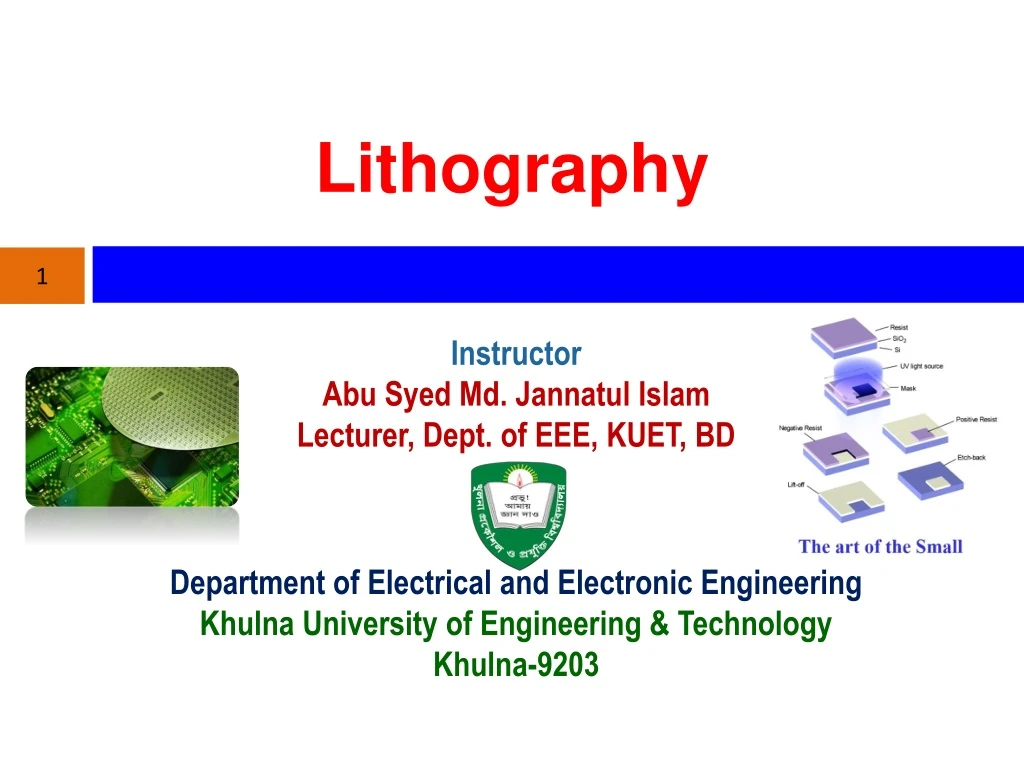
Lithography 1 • Instructor • Abu Syed Md. JannatulIslam • Lecturer, Dept. of EEE, KUET, BD • Department of Electrical and Electronic Engineering • Khulna University of Engineering & Technology • Khulna-9203
Why Lithography? 5 • Simple layers of thin films do not make a Device.
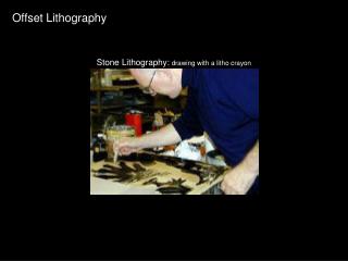
History of Lithography 7 • It was invented in 1796 by German author and actor Alois Senefelder as a cheap method of publishing theatrical works.
What is Lithography ? 8 • Lithography comes from two Greek words, “lithos” which means stone and “graphein”which means write. • “ writing a pattern on stone” • Lithography is the transfer of geometric shapes on a mask to a smooth surface • It uses light or other forms of radiant energy to change the chemical properties of thin layers of films that have been coated on a substrate. • Typically 8-25 lithography steps and several hundred processing steps between exposure are required to fabricate a packed IC.
What is lithography ? 9 Lithography is one of the 4 major processes in the top-down model Lithography Etching Deposition Doping • In order to perform the other 3 processes, • we must precisely define where to do them • Lithography Does This!
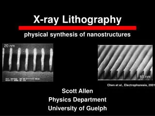
Types of Lithography 10 • Photolithography • E-beam lithography • X-ray lithography. • Interference lithography. • Scanning Probe lithography
Photolithography 11 Photolithography is the process of transferring patterns of geometric shapes on a mask to a thin layer of photosensitive material (called photoresist) covering the surface of a semiconductor wafer. • A light sensitive photoresist is spun onto the wafer forming a thin layer on the surface. • The resist is then selectively exposed by shining light through a mask which contains the pattern information for the particular being fabricated. • The resist is then developed which completes the pattern transfer from the mask to the wafer.
Photolithography 12 Photolithography is an optical means for transferring patterns onto a substrate Overview of the Photolithography Process Surface Preparation (Get rid of H2O, RCA clean, apply adhesion promoter Deposit (Photoresist Coating by Spin Casting) Soft Bake(90 – 120°C for 60 –120 sec to remove solvent from liquid photoresist Photo Mask Alignment Exposure (Pattern transfer) Development (Remove soluble photoresist) Hard Bake (100 – 180°C) to increase adhesion Etching (Remove oxide) Stripping (Photoresist removal) Post Processing/Cleaning (Ashing)
Photolithography 13 Grow Oxide Layer
Photolithography 14 Add Photoresist
Photolithography 15 Photo-Mask
Photolithography 16 UV Exposed to Photomask to transfer pattern
Photolithography 17 Remove Photoresist
Photolithography 18 Remove the oxide using Etching
Photolithography 19 Now remove the photo resist by ashing
Photolithography 20 Diffuse new region by ion implantation or diffusion
Photolithography 23 The surface patterns of the various integrated-circuit components can be defined repeatedly using photolithography Here, a photographic plate with drawn patterns will be used to selectively expose the photoresist under a deep ultraviolet illumination (UV) The exposed areas will become softened (for positive photoresist) The exposed layer can then be removed using a chemical developer, causing the mask pattern to be duplicated on the wafer Silicon dioxide, silicon nitride, polysilicon, and metal layers can be selectively removed using the appropriate etching methods After the etching step(s), the photoresist is stripped away, leaving behind a permanent pattern of the photomask on the wafer surface
Photoresist Coating 25 The wafer surface is coated with a photosensitive layer called photoresist, using a spin-on technique
Photoresist Composition 27 • The most commonly used positive resist consist of diazonaphtoquinone (DQ), which is the photoactive compound (PAC), and novolac (N), a matrix material called resin. Upon absorption of UV light, the PAC undergoes a structural transformation which is followed by reaction with water to form a base soluble carboxylic acid, which is readily soluble in basic developer (KOH, NAOH, TMAH etc.)
Types of Photoresist 28 • Positive Photoresist • Most commonly used in the IC industry. • Become soluble after exposure • Better resolution • Cheaper • Negative Photoresist • Becomes insoluble after exposure • When developed, the unexposed parts dissolved • Cheaper
Soft Bake 29 • Used to evaporate the coating solvent and to densify the resist after spin coating. • Typical thermal cycles: 90-100°C for 20 min. in a convection oven, 75-85°C for 45 sec. on a hot plate • Commercially, microwave heating or IR lamps are also used in production lines. • Improves adhesion • Improves uniformity • Improves etch resistance • Improves line width control • Optimizes light absorbance characteristics of photoresist
What Is a Photomask? 30 • Photomasks are high precision plates containing microscopic images of electronic circuits. Material Used to make Photomasks: • There are four types of material used to make photomasks; • quartz (the most commonly used and most expensive), LE, soda lime, and white crown.
Different Photomasks 32 • 15 – 20 different mask levels are typically required for a complete IC process
Light Sources 35 Increasing Cost
Contact Printing 38 • The mask is directly in contact with the wafer • Advantages • Simple • Low Cost • Disadvantages • Poor for small features • Mask damage may occur from contact • Defects from contaminants on mask or wafer due to contacting surfaces
Proximity Printing 39 • The mask is above the wafer surface • Advantages • Mask damage is minimal • Good registration possible • Disadvantages • Poorer resolution due to distance from the surface • Diffraction errors
Projection Printing 40 • An optical system focuses the light source and reduces the mask image for exposure on the surface • Advantages • Higher resolution • Lens system reduces diffraction error • Disadvantages • Errors due to focus of lens system may occur • Limiting factor in resolution can be due to optical system
developer dispenser vacuum chuck to vacuum pump spindle Develop 41 • Soluble areas of photoresist are dissolved by developer chemical • Visible patterns appear on wafer • windows • islands
Hard Bake 42 • Evaporate remaining photoresist • Improve adhesion • Used to stabilize and harden the developed photoresist prior to processing steps • Eliminates the solvent burst effects in vacuum processing • Introduces some stress into the photoresist. • Needed for acid etching, e.g. BOE.
Etching 43 • Etch oxide with hydrofluoric acid (HF) • Only attacks oxide where resist has been exposed
Photoresist Removal (Stripping) 44 • Want to remove the photoresist and any of its residues. • – Positive photoresists: • • acetone • • trichloroethylene (TCE) • • phenol-based strippers • – Negative photoresists: • • methyl ethyl ketone (MEK), CH3COC2H5 • • methyl isobutyl ketone (MIBK), CH3COC4H9 Plasma etching with O2(Ashing) is also effective for removing organic polymer debris.
Performance Metrics 45 • Resolution: minimum feature dimension that can be transferred with high fidelity to a resist film. • Registration: how accurately patterns on successive masks can be aligned (or overlaid) with respect to previously defined patterns. • Throughput: number of wafers that can be exposed/unit time for a given mask level.
Limitations of Optical Lithography 46 • Resolution becoming a challenge for deep-submicron IC process requirements • Complexity of mask production and mask inspection • High cost of masks
Electron Beam Lithography 47 • Involves direct exposure of the resist by a focused electron beam without a mask • Resolution as low as 10 – 25 nm
Electron Beam Lithography 48 • Electron gun generates beam of electrons • Condenser lenses focus the e-beam • Beam-blanking plates turn beam on and off
Electron Beam Lithography 49 • Advantages • Generation of submicron resist geometries • Highly automated and precisely controlled operation • Greater depth of focus than that available from optical lithography • Direct patterning on wafer without using a mask • Disadvantages • Low throughput • Expensive resists • Proximity effect: backscattering of electrons irradiates adjacent regions and limits minimum spacing between features
Extreme ultraviolet : EUV 50 Next Generation Lithography • Vacuum operation • Laser plasma source • Very expensive system • Uses very short 13.4 nm light • Step and scan printing • All reflective optics (at this wavelength all materials absorb!) • Uses reduction optics (4X) • Optical tricks seen before all apply: off axis illumination (OAI), phase shift masks and OPC