Download
1 / 26
270 likes | 464 Vues
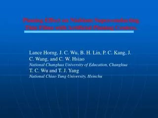
Pinning Effect on Niobium Superconducting Thin Films with Artificial Pinning Centers. Lance Horng, J. C. Wu, B. H. Lin, P. C. Kang, J. C. Wang, and C. W. Hsiao National Changhua University of Education, Changhua T. C. Wu and T. J. Yang National Chiao Tung University, Hsinchu. OUTLINE.

E N D
Pinning Effect on Niobium Superconducting Thin Films with Artificial Pinning Centers. Lance Horng, J. C. Wu, B. H. Lin, P. C. Kang, J. C. Wang, and C. W. Hsiao National Changhua University of Education, Changhua T. C. Wu and T. J. Yang National Chiao Tung University, Hsinchu
OUTLINE • 1.Motivation • 2.Experimental methods: • Fabrication – electron beam lithography • Measurement – four-probe measurement • 3.Results and Analysis • Artificial pinning arrays of pinning sites Square arrays Triangular arrays Honeycomb arrays • 4.Conclusions
B I I Schematic drawing for flux flowing
Fabrication A B C E-beam Writing Development RIE etching Si3N4 D E Nb films Si Opening cross trenches in PMMA Nb sputtering Cross section
Keithley-182 Keithley-224 樣品位置
Square arrays of pinning sites AFM image of the patterned films Field dependence of the resistance and critical current for a Nb film with a square array of defects at T=8.75 K. J. Appl. Phys. 91, 8510 (2001) Jpn. J. Appl. Phys.42, 2679 (2003)
Molecular dynamics simulations of vortex states Vortex configurations at integer matching fields in square pinning array C. Reichhardt et al., Phys. Rev. B 57, 7937 (1998)
Triangular arrays of pinning sites AFM image of the Nb films Magnetoresistance curves taken at T = 8.73 K for different currents for this sample.
I-V characteristics for a triangle lattice at T=8.73 K under various magnetic fields applied perpendicular to the film plane.
Schematic of the current geometry relative to the rhombic unit cell. SEM micrograph of the patterned sample.
Critical current as a function of the magnetic field for a Nb film with a triangular array of defects.
The vortices distribution (filled circles) and pinning sites (open circles) for (a) the incommensurate row and (b) the interstitial flowing channel.
a a
SEM micrograph of the patterned sample. The honeycomb array of corrugated holes with spacing of 400 nm and hole diameter of around 200nm embedded in the 100 nm thick superconducting Nb thin films AFM image of the patterned sample. The depth of holes is around 70 nm
n = 0.5 n = 1.5 n = 1.0 n = 3.5 n = 2.0 n = 3.0 n = 2.5 Schematic of the Vortex states that are possible for n = B / ∆B = 0.5, 1.0, 1.5, 2.0, 2.5, 3.0, and 3.5.
Conclusion • Flux-line confinement by a array of sub-micrometer holes has been studied in a superconducting Nb film of corrugated pinning sites. • The matching effects observed in the MR and Ic(H) curves are related to the flux pinning caused by the array of defects. • The interplay between nanostructured superconductors and Abrikosov vortex lattice is a powerful tool to explore motion of particles in different scenarios.