
1. SDRAM 이란 ?
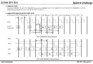
1. SDRAM 이란 ? Syncronous DRAM 으로 일반적인 DRAM 과 (Asyncronous DRAM) 는 달리 외부 CLK 에 동기되어 동작하므로 SDRAM 이라고하며 , CLK 의 Rising Edeg 에 동기되어 모든 동작이 일어 나게된다 . 2. SDRAM 과 EDO RAM 과의 동작 비교 - 실제 System 상에서의 Performace 증가는 수 % 에 불가 : Cach Memory 가 없는 경우 :4~6%, Cach Memory 가 있는 경우 1~2%.

1. SDRAM 이란 ?
E N D
Presentation Transcript
1. SDRAM 이란? Syncronous DRAM으로 일반적인 DRAM과(Asyncronous DRAM)는 달리 외부 CLK에 동기되어 동작하므로 SDRAM이라고하며, CLK의 Rising Edeg에 동기되어 모든 동작이 일어 나게된다. 2. SDRAM과 EDO RAM과의 동작 비교 - 실제 System 상에서의 Performace 증가는 수 %에 불가 : Cach Memory 가 없는 경우 :4~6%, Cach Memory 가 있는 경우 1~2% tCK CLK tAC 이외의 Control Pin D3 D2 C D1 R D0 CL=2 BL=4 (Burst Length) (CAS Latency) 그림1. SDRAM의 Timing Diagram /RAS tCP /CAS C3 Add C0 C2 R C1 Dout D3 D2 D1 D0 그림2. EDO DRAM의 Timing Diagram
3. Pin Configuration 4. Pin Name VSS CLK CKE /CS /RAS /CAS /WE A0~A9,A11 A10 / AP BA0/A13 ~BA1/A12 DQ0~DQ15 DQMU/DQML VCCQ VSSQ VCC VSS NC Clock Clock Enable Chip Select Row Address Strobe Column Address Strobe Write Enable Address input Address input or Auto Precharge Bank select Data input / Data output Data input / output Mask VCC for DQ VSS for DQ Power for internal circuit Ground for internal circuit No Connection VCC DQ15 DQ0 VSSQ VCCQ DQ14 DQ1 DQ13 DQ2 VCCQ VSSQ DQ12 DQ3 DQ11 DQ4 VSSQ VCCQ DQ10 DQ5 DQ9 DQ6 VCCQ VSSQ DQ8 DQ7 VSS VCC NC DQML DQMU /WE CLK /CAS CKE /RAS NC /CS A11 BA0/A13 A9 BA1/A12 A8 A10,AP A7 A0 A6 A1 A5 A2 A4 A3 VSS VCC
out 0-1 out 0 out 1 CAS Latency CLK tRCD Command ACTV READ Address Row Column out 0 out 1 out 2 out 3 CL = 2 Dout out 0 out 1 out 2 out 3 CL = 3 CL : CAS Latency Burst Length = 4 Q1. SDRAM에서의 가장 기본적인 내용은 무엇인가요? 글쎄요? 아마도 CAS Latency와 Burst Length가 아닐 런지요. 일반 적인 DRAM에서는 없던 것으로 결국 SDRAM을 이해하는 중요한 단어 입니다. CAS Latency라 불리는 것은 말 Read시 몇개의 CLK가 지나간 후에 원하는 Data를 얻을 수 있는가를 표시하는 단어입니다. 일반적으로 CL=2또는 3이 사용되며, CL=1에서는 마치 DRAM의 동작과 유사하여 P검등 Test시에 사용을 하고 있읍니다. 하지만 불행하게도 SDRAM에서 Write시에는 CL=0입니다. Burst Length라는 것은 한번 읽고 쓰는 단위가 몇개 인가를 나타내는 단위입니다. Burst Length CLK tRCD Command Active Read Address Row Column out 0 BL = 1 out 0 out 1 BL = 2 out 0 out 1 out 2 out 3 BL = 4 Dout out 0 out 1 out 2 out 3 out 4 out 5 out 6 out 7 BL = 8 out 0 out 1 out 2 out 3 out 4 out 5 out 6 out 7 out 8 BL = Full Page BL = Burst Length CAS Latency = 2
A6 A5 A4 CAS Latency A2 A1 A0 Burst Length 0 0 0 R BT=0 BT=1 0 0 1 R 0 0 0 1 1 0 1 0 2 0 0 1 2 2 0 1 1 3 0 1 0 4 4 1 X X R 0 1 1 8 8 1 0 0 R R 1 0 1 R R 1 1 0 R R A13 A12 A11 A10 A9 A8 Write mode 1 1 1 F.P. R 0 0 0 0 Burst read and BURST WRITE 0 0 X X X X 0 1 R X X X X 1 0 Burst read and SINGLE WRITE X X X X 1 1 R MRS Setting Q1. SDRAM은 Mode Register를 Setting 해야 된다는데? 맞습니다. SDRAM은 Power가 켜진 후에 반드시 Mode Register를 Setting 해 주어야 합니다. 이유는 SDRAM 내부에는 처음에 이야기한 CL,BL및 몇가지의 내용을 사용전에 알려 주어야만 사용자가 원하는데로 사용이 가능하도록 되어 있읍니다. 이것은 많은 사용자가 자기가 원하는 Mode로 사용 가능하도록 하기 위해 여러가지 Mode를 미리 준비해 둔 것입니다. 그러면 어떻게 사용하는지 알아 봅시다. A13 A12 A11 A10 A9 A8 A7 A6 A5 A4 A3 A2 A1 A0 OPCODE 0 LMODE BT BL A3 Burst Type 0 Sequential 1 Interleave CLK /CS /RAS /CAS /WE MRS Setting Cycle 여러가지 Mode를 Setting하게됨.(BL,CL등)
The synchronous DRAM recognizes the following commands specified by the CS, RAS, CAS, WE and address pins. CKE A12~A13 A0~ A11 Function Symbol CS RAS CAS WE A10 n n-1 Ignore command DESL H X H X X X X X X NOP H X L H H H X X X No Operation BST H X L H H L X X X Burst stop in full page Column address and read command READ H X L H L H V L V READ A H X L H L H V H V Read with auto-precharge Column address and write command WRIT H X L H L L V L V WRIT A H X L H L L V H V Write with auto-precharge Row address strobe and bank active ACTV H X L L H H V V V PRE H X L L H L V L X Precharge select bank PALL H X L L H L X H X Precharge all banks REF/SELF H V L L L H X X X Refresh MRS H X L L L L V V V Mode register set Command Truth Table Q1. SDRAM의 Command에는 어떤 것들이 있는지요? A. 우선 가장 먼저 SDRAM은 Memory라는 것을 기억해야합니다. 따라서 Command도 대부분이 Memory Cell을 읽고 쓰기 위한 것입니다. 즉 READ,WRITE 동작을 하기위한 것입니다. 또한 Dynamic이므로 Memory 이므로 Refresh를 해주어야 기억된 정보를 잊어 버리지 않으므로 이것과 관련된 Command가 필요합니다. 기본적으로는 위의 2가지 정도로 충분하지만 좀 더 깊이 들어가면 SDRAM 내부는 복수개의 Bank로 구성되어져 있읍니다. 이 Bank라는 것이 마치 하나의 단위 Memory 처럼 동작이 가능합니다. 따라서 상호 Bank간의 Read, Write가 가능해지므로 인해 Bank Interrupt라는 좀 어려운 이야기가 나오게 됩니다. * Notes : H: VIH, L: VIL, X: VIH or VIL, V: Valid address input
SELF- REFRESH SDRAM 동작표 SR ENTRY SR EXIT MODE REGISTER SET MRS AUTO- REFRESH *1 IDLE REFRESH CKE=L IDLE POWER DOWN ACTIVE CLOCK SUSPEND CKE=H ACTIVE CKE=L CKE=H ROW ACTIVE BST (on full page) WRITE BST (on full page) READ WRITE WITH AP Write Read READ WITH AP CKE=L WRITE SUSPEND WRITE READ SUSPEND CKE=L READ READ WRITE CKE=H READ WITH AP CKE=H READ WITH AP WRITE WITH AP WRITE WITH AP WRITEA SUSPEND CKE=L WRITEA CKE=L READA SUSPEND READA PRECHARGE PRECHARGE PRECHARGE CKE=H CKE=H PRE- CHARGE POWER ON POWER APPLIED PRECHARGE Automatic Transition after completion of command. Transition resulting from command input.
out 0-1 out 0 out 1 Burst Write Q1. 그럼 실제 Read Write 동작을 설명해 주세요? A. CL=2, BL=4로 MRS가 Setting되어 있다고 가정 합시다. Write시에는 1) Data를 저장할 X-Address가 지정되어야합니다. 이것을 수행하는 Command가 ACTV로 Word Line을 Active 시키고, 이것에 연결된 Sense Amp를 Enable시켜 저장된 Data Sense Amp가 Develop하여 가지고 있게 됩니다. 2) tRCD Timing후에(여기서 tRCD는 X계 관련된 신호가 처리된 후 Y계 신호가 처리 될 수 있도록 필요한 시간) Write하기 위한 WRIT Command가 입력되면서 Write할 Y-Address가 A0~A9, Data가 DQ0~DQ15까지 입력 되면 4개의 Data가 순서대로 Memory Cell에 써지게 됩니다. 3) 이것이 완료된 후 Precharge Command가 입력되면 Write 동작이 완료 됩니다. Read시에는 Write시와 동일하게 1)이 수행되며, 2)에서 CL=2만큼 CLK후에 Data를 출력하게 된다. 3)에서 Precharge를 수행하게 된다. CLK tRCD Command ACTV WRIT Address Row Column in 0 BL = 1 in 0 in 1 BL = 2 in 0 in 1 in 2 in 3 BL = 4 Din in 0 in 1 in 2 in 3 in 4 in 5 in 6 in 7 BL = 8 in 0 in 1 in 2 in 3 in 4 in 5 in 6 in 7 in 8 in 9 in 10 in 11 in 0-1 in 0 in 1 BL = Full Page CAS Latency = 2, 3 Burst Read CLK tRCD Command Active Read W/L Address Row Column out 0 BL = 1 out 0 out 1 B/L BL = 2 out 0 out 1 out 2 out 3 BL = 4 Dout out 0 out 1 out 2 out 3 out 4 out 5 out 6 out 7 BL = 8 out 0 out 1 out 2 out 3 out 4 out 5 out 6 out 7 out 8 BL = Full Page BL = Burst Length CAS Latency = 2
Q1. SDRAM의 Precharge 동작에 대해 알려 주세요. READ to PRECHARGE Command Interval (same bank) : To output all data WRITE to PRECHARGE Command Interval (same bank) CAS Latency = 2, Burst Length = 4 CAS Latency = 2, Burst Length = 4 CLK CLK Command Command READ PRE/PALL WRIT PRE/PALL Dout Din out A0 out A1 out A2 out A3 in A0 in A1 in A2 in A3 tRWL lEP = -1 Cycle CL=2 CAS Latency = 3, Burst Length = 4 CAS Latency = 3, Burst Length = 4 CLK CLK Command Command READ PRE/PALL WRIT PRE/PALL Dout Din out A0 out A1 out A2 out A3 out A0 out A1 out A2 out A3 tRWL CL=3 lEP = -2 Cycle
READ to READ Command Interval (Same Row Address in Same Bank) READ to READ Command Interval (different bank) WRITE to WRITE Command Interval (different bank) CLK CLK CLK Command ACTV READ READ Command ACTV ACTV WRIT WRIT Command ACTV ACTV READ READ Address (A0-A11) Address (A0-A11) Address (A0-A11) Row 0 Row 1 Column A Column B Row 0 Row 1 Column A Column B BS(A12/A13) BS(A12/A13) WRITE to WRITE Command Interval (same ROW address in same bank) BS(A12/A13) Dout out A0 out B0 out B1 out B2 out B3 CLK Dout Din out A0 out B0 out B1 out B2 out B3 in A0 in B0 in B1 in B2 in B3 Bank0 Active Column=A Read Column=B Read Column=A Dout Column=B Dout CAS Latency =3 Burst Length = 4 Bank0 Burst Write Mode Burst Length = 4 Bank0 Active Bank3 Active Bank0 Read Bank3 Read Bank0 Dout Bank3 Dout Bank0 Active Bank3 Active Bank0 Write Bank3 Write CAS Latency = 3 Burst Length = 4 Command ACTV WRIT WRIT Address (A0-A11) Row Column A Column B Row Column A Column B BS(A12/A13) Din in A0 in B0 in B1 in B2 in B3 Burst Write Mode Burst Length = 4 Bank0 Bank0 Active Column=A Write Column=B Write Q1. Bank Interrupt Operation을 설명해 주세요.
개발 제품의 Target Spec. 예 항 목 제품 A 제품 B 제품 C 4M Bit x 4I/O x 4Bank, 8M Bit x 4I/O x 2Bank Bit Organization 2M Bit x 8I/O x 4Bank, 4M Bit x 8I/O x 2Bank 1M Bit x 16I/O x 4Bank, 1M Bit x 16I/O x 2Bank No x16 167/143/133/125MHz Max Clock 133MHz(@CL=2) 133MHz(@CL=3) 6.0ns/7.0ns/7.5ns Clock Cycle Time Access Time tAC= 5.4ns(@CL=2) tAC= 5.4ns(CL=3) Refresh Cycle/Time Auto: 4K Cycle/64ms External : VDD = 3.3V ±0.3V Power Supply Internal : VPERI = 2.5V, VDL = 1.8V VDL = 2.0V Interface LVTTL only Bank 2Bank / 4Bank Mask Option Bonding Option Option Bit x4/x8/x16 Bonding x4/x8 Bonding CAS Latency : 1/2/3 Burst Length : 1/2/4/8/Full Page with BST Function Burst Type : Sequential Type/Interleave Type Write Type : Single Write Capability Data Mask : DQM or DQML/DQMU DQM DC Spec. 상세Spec 참조 TBD tAC=5.4ns,tRAC=35.4ns PC133 AC Spec. (133/125/100MHz) tRAS=45/48/50ns,tRCD=20ns,tRP=20ns,tRWL=15/20/20ns 상세Spec 참조 tOH=2/2/3ns, tS=1.5/2/2ns, tH=0.5/1/1ns
아사 제품의 SDRAM Architecture X-Redundancy(MWD기준) Y-Redundancy(YS기준) (0,0) (0,0) Y-Address증가 Y-Address증가 Bank0 Bank2 Main Word Driver Main Word Driver X-Address증가 Y-DEC(1of 256) Y-DEC(1of 256) 128K Bit 단위 MAT M/A(4ea) M/A(4ea) M/A(4ea) M/A(4ea) M/A(4ea) M/A(4ea) M/A(4ea) M/A(4ea) M/A(4ea) M/A(4ea) M/A(4ea) M/A(4ea) M/A(4ea) M/A(4ea) M/A(4ea) M/A(4ea) 2K Disturb Test를 위한 X-Redundancy Y-DEC(1of 256) Y-DEC(1of 256) X-Address증가 Bank1 Bank3 Main Word Driver Main Word Driver (0,0) (0,0) Y-Address증가 Y-Address증가
향후 SDRAM의 개발 진행 방향은 ? 1. 고속화 1) 고속화를 위해서는 tCK를 줄여서 동작 주파수를 높이는 방법. 예) 66MHz --> 100MHz --> 125Mhz --> 133MHz --> 166Mhz --> 200MHz 2) tRCD, CL등을 줄이는 방법. 예) 20ns tRCD를 2 CLK에 완성하기 위해 16ns로 줄임. CL=3를 CL=2로 하여 1CLK의 이득을 가짐. 3) SDRAM에서 CLK의 Rising Edge에서의 동작을 Falling Edge에서도 동작이 이루어지도록함. 예) 현재 개발 진핸중인 DDR SDRAM (Double Data Rate SDRAM)으로 Rising, Falling Edge 모두에서 동작이 이루어짐. 2. 저전력화 1) 휴대용 PC등의 Battery Backup이 가능하도록 저전력 사용이 필수적임. 2) 복수개의 Bank Enable에 대한 Refresh Current 저감.