Download
1 / 40
650 likes | 1.27k Vues
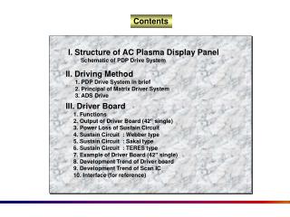
Contents. I. Structure of AC Plasma Display Panel Schematic of PDP Drive System. II. Driving Method 1. PDP Drive System in brief 2. Principal of Matrix Driver System 3. ADS Drive. III. Driver Board 1. Functions 2. Output of Driver Board (42” single)

E N D
Contents I. Structure of AC Plasma Display Panel Schematic of PDP Drive System II. Driving Method 1. PDP Drive System in brief 2. Principal of Matrix Driver System 3. ADS Drive III. Driver Board 1. Functions 2. Output of Driver Board (42” single) 3. Power Loss of Sustain Circuit 4. Sustain Circuit : Webber type 5. Sustain Circuit : Sakai type 6. Sustain Circuit : TERES type 7. Example of Driver Board (42” single) 8. Development Trend of Driver board 9. Development Trend of Scan IC 10. Interface (for reference)
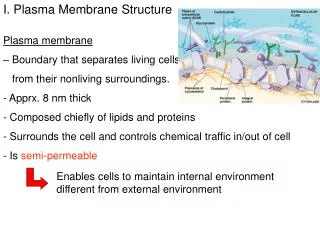
Front Glass Dielectric Layer X, Y Electrode MgO Layer PDP TV Barrier Rib IONs Electrons Rear Glass Phosphor Address Electrode + + + + - - - - Structure of PDP Discharge Discharge in the PDP cell I. Structure of AC Plasma Display Panel
Address System Address Power Source D1 D2 D3 D4 D5 Y1 Y2 X Y3 ○ Each cells are selected by switch “On” of Address Electrodes. ○ Discharge for display is operated by switch “On” of Y-port(Scan) and X-port(Sustain) by turns. Y4 Y5 Sustain Power Source Scan Power Source I. Structure of AC Plasma Display Panel Schematic of PDP Drive System
ON Y3 Y2 OFF Y1 X1 X2 X3 II. Driving Method 1. Principal of Matrix Driver System
ON Y3 Y2 OFF Y1 X1 X2 X3 2. Driving Method Principal of Matrix Driver System
SF1 SF2 SF3 SF4 SF5 SF6 SF7 SF8 sub-field 1 2 address scan line ..... 1T 2T 4T 8T 16T 32T 64T 128T sustain 480 1TV field (time) Reset Period Address Period Sustain Period D X Y1 Y2 Yn II. Driving Method 2. Structure of ADS Drive Method Gray scale is displayed by s/w ‘On’ of specific SF(sub field) in 1TV frame(field time).
II. Driving Method 3. Feature of ADS Drive Pulse • (Terminology) • Reset : Elimination of Sustain discharge / • Formation of Address discharge’s condition • Address : Selection of ON/OFF Cell • Sustain : Display real picture through Sustain discharge • Time : In case of Dual Scan (480 scan line), 1 Frame (16.67msec) are organized • Reset 15 ~ 20%, Address 40 ~ 50% and Sustain 35 ~ 40%.
Address Operation In order to display picture, select the cells.
Sustain operation Display cells through strong Sustain discharge.
Erase / Reset Elimination for next image (generate Display discharge)
III. Driver Board 1. Functions Disposition of Boards Address Buffer Board (upper) Logic Board Power Supply Board Y Electrode X Electrode Image Processing Board X-B’d Y-B’d Address Buffer Board (Lower) Scan-B’d Sustain pulse generation Reset pulse generation Scanning operation Basic signal protection Short circuit protection Main functions = +
III. Driver Board Y- Board Power & Signal Flow Switch On / Off Reset / Scan Wave Reset / Scan Volts AC Power Switch On / Off Sustain Volts Sustain Wave Filter Logic Volts Scan Buffer Capacitor FET Drive Volts Y - Electrode Logic Board Logic Signal
III. Driver Board X- Board Power & Signal Flow Switch ON/OFF X-bias X-bias Volts AC Power Switch ON/OFF Sustain Volts Sustain Wave Filter Logic Volts Capacitor FET Drive Volts Y - Electrode Logic Board Logic Signal
Vth Current of Resonance Ipk : 60-70A Current of Discharge Ipk : 120A-150A III. Driver Board 2. Output of Driver Board (42” Single) Addressing => Address period is long Sustain Discharge Luminescence part • Reset • Ramp Reset • (weak discharge reset) • Contrast, operation margin, expanded production rate
address pulse Ai ~ ~ ~ ~ sustain pulse self-erase pluse ~ ~ X ~ ~ erase pluse Yj scan pulse ~ ~ ~ ~ time reset period address period sustain period III. Driver Board 2. Output of Driver Board(42” Dual Scan) : Reference Dual Scan (Address period is short) LOG Reset Wave in use • The point of view on Driver board, Dual Scan is same structure with Single Scan except the circuit • of Reset Wave output.
Front Glass Dielectric Layer X, Y Electrode MgO Layer Barrier Rib Rear Glass Phosphor Address Electrode Electrical model = Capacitor III. Driver Board 3. Power Loss of Sustain circuit PDP Structure Basic sustain circuit PDP panel
III. Driver Board PDP Discharge of Capacity load Heat loss Heat loss Power loss= About 120 Watts in case of 42inch panel C : panel capacitance V: sustain voltage f: average frequency
III. Driver Board 4. Sustain Circuit : Webber type Y-Board X-Board Panel Sustain circuit Energy’s Recovery circuit Energy’s Recovery circuit • Operation performance of this circuit is good. (compatible with most Waves) • Overall efficiency is high. (On the usage of LC Resonance circuit, switching loss should be small.) • Simple operation and organization. Operation is stable. • Production enterprise with Webber type : Matsushita, Fujits, Pioneer, LG, Samsung Characteristics
III. Driver Board Hard switching generation 1. Rising period Ys,Xg Yr,Xg Yf,Xg Yg,Xg 2. Vs - Sustain period Sustain Wave Y X Light Wave Observation Wave
III. Driver Board Hard switching generation 3. Falling period Ys,Xg Yf,Xg Yr,Xg Yg,Xg 4. GNDperiod Sustain Wave Y X Light Wave Observation Wave
III. Driver Board 5. Sustain Circuit : Sakai type Y-Board X-Board Panel Energy Recovery circuit • Operation performance of this circuit is low. • (It is not proper to recover the energy except Sustain part.) • Overall efficiency is high. (On the usage of LC Resonance circuit, switching loss should be small.) • Simple operation and organization. Operation is stable. • Production enterprise with Sakai type : NEC Characteristics
III. Driver Board Hard switching generation 1. Y rising & X falling period Sa Ys,Xg Xs,Yg Sb Sustain Wave Ys,Xg Yr,Xg Yf,Xg Yg,Xg 2. Sustain period X Y Observation Wave
III. Driver Board Hard switching generation 3. X rising & Y falling period Sa Ys,Xg Xs,Yg Sb Sustain Wave Ys,Xg 4. Sustain period X Y Observation Wave
III. Driver Board 6. Sustain Circuit : TERES type Panel Charge pump방식 • TERES type hold a patent right for the structure of Sustain circuit. • It is advantage of low price. (low voltage part in use) • Complicated operation and organization. • It should be added ERC circuit like Sakai type or Webber type. • Production enterprise with TERES type : FHP Characteristics
III. Driver Board Sustain path Vy Vx Charge pump path Vy Vx Internal voltages of Device : ½ comparing with the other type Performance : same as the other type Cost : profitable comparing with the other type Application : It is not compatible with every Waves ( swing +,- by turns) Sustain path Charge pump path
III. Driver Board 7. Example of Driver Board ( 42” single ) Ysc Dyvs ERC circuit (Yr,Yf,Dyys,Dyr,Dyf,Dyg) => Energy recovery Sustain circuit (Ys, Yg) => Sustain Discharge Reset circuit (Yrr, Yfr) => Elimination of Panel Path circuit (Yp, Ysp) => Formation of Main Path Scan circui t(Ysc) => Scan Bias Yrr Ys Yp Dyr Yr Dyf Yp Yg Ysp Yf Dyg Yfr Y-Board
III. Driver Board Xrr • ERC circuit (Xr, Xf, Dxvs, Dxr, Dxf, Dxg) • => Energy recovery Dxvs Xf • Sustain circuit (Xs, Xg) • => Sustain Discharge Dxf Xs • Reset circuit (Xrr) • => Elimination of Panel Xr Dyf Dxr Xg Dxg X-Board
III. Driver Board 42” single Scan Buffer Y-BRD X-BRD SMPS Logic Address Buffer
III. Driver Board 50” Dual Scan Buffer Address Buffer Y-BRD X-BRD SMPS Logic Address Buffer * The Load of Driver Board(50”) is about 1.5 times bigger than 42”’s.
III. Driver Board 50” Dual Clamping Diode Clamping Diode Ysc Xf Xs Ys Yr Yp Ysp Xrr Yf Xr Yg Xg Yrr Yfr Blocking Diode
III. Driver Board Circuit Block Diagram Path circuit(Yp, Ysp) Scan circuit(Ysc) Sustain circuit (Xs, Xg) Sustain circuit (Ys, Yg) Reset circuit (Yrr, Yfr, Xrr) ERC circuit (Yr, Yf, Dyvs, Dyr, Dyf, Dyg) ERC circuit (Xr, Xf, Dxvs, Dxr, Dxf, Dxg)
III. Driver Board Operations(Sustain part) (2) (1) (4) (3) Yp, Ysp : ON
III. Driver Board Operations (Reset part) (2) (1),(4) (2) Regarding rising points and falling points of Ramp Wave, use Sustain operations.
III. Driver Board Operations (Scan part)
III. Driver Board Operations (Scan part) 768 line scan t=t0 t=t1 480 line t=t2 t=t3 GND t=t0 t=t1 Address t=t2 t=t3
Vth III. Driver Board Path Diode Path Diode Discharge Current Ipk : 120A-150A pulse width : 1us미만 Resonance Current Ipk : 60-70A pulse width : 300-400 ns Parallel position of Switch and Diode X-BRD Y-BRD ERC S/W Sustain S/W Sustain & Path S/W ERC S/W
Examples of Operation Wave III. Driver Board Matsushita Samsung Matsushita NEC
III. Driver Board 8. Development Trend of Driver board • Improvement ofBoard efficiency and Design for radiation of heat • : Decline of Board’s electric power consumption and Operations • of Fanless motor for the radiation. • Thickness Low depth • : Dignity elivation of the set • Design for Low Cost • a. Development of new part • b. Change of Circuit Topology • c. Design change in accordance with Operation Wave change • Application of HIC (Hybrid Intergrated Circuit) • : PCB Size decline, Improvement of Production process , • Development and Application trend in each PDP’s vendor • Development for self Operation type except a patent right for Webber
III. Driver Board 9. Development Trend of Scan IC • Scan IC / Address IC • a. Low Coat • Development of Low Voltage Address Operation type • through change of Operation Wave • ⇒ Application of Low Voltage Driver • b. High Speed • Needs the Data processing quickly for the • reduction of Address Cycle • ⇒ Speedy Data Shift Clock
III. Driver Board 10. Interface (for reference) • Connection of the circuit output and Panel • : usage the FPC (Flexible Printed Circuit) • Connection of Scan/Address Driver and Panel • : On the usage of FPC, Boards are connected with • Panel electrode. • a. Board + Connector + FPC + Panel • b. COB(FPC) + Panel • c. COF(FPC) + Panel • Trend changes to COB / COF type on overall • PDP manufacturing vendors. Example : FPC(Flexible Printed Circuit)