Lecture 26 Logic BIST Architectures
270 likes | 481 Vues
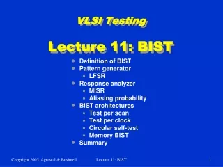
Lecture 26 Logic BIST Architectures. Motivation Built-in Logic Block Observer (BILBO) Test / clock systems Test / scan systems Circular self-test path (CSTP) BIST Circuit initialization Loop-back hardware Test point insertion Summary. Motivation.

Lecture 26 Logic BIST Architectures
E N D
Presentation Transcript
Lecture 26Logic BIST Architectures • Motivation • Built-in Logic Block Observer (BILBO) • Test / clock systems • Test / scan systems • Circular self-test path (CSTP) BIST • Circuit initialization • Loop-back hardware • Test point insertion • Summary VLSI Test: Bushnell-Agrawal/Lecture 26
Motivation • Complex systems with multiple chips demand elaborate logic BIST architectures • BILBO and test / clock system • Shorter test length, more BIST hardware • STUMPS & test / scan systems • Longer test length, less BIST hardware • Circular Self-Test Path • Lowest hardware, lower fault coverage • Benefits: cheaper system test, Cost: more hdwe. • Must modify fully synthesized circuit for BIST to boost fault coverage • Initialization, loop-back, test point hardware VLSI Test: Bushnell-Agrawal/Lecture 26
Built-in Logic Block Observer (BILBO) • Combined functionality of D flip-flop, pattern generator, response compacter, & scan chain • Reset all FFs to 0 by scanning in zeros VLSI Test: Bushnell-Agrawal/Lecture 26
Example BILBO Usage • SI – Scan In • SO – Scan Out • Characteristic polynomial: 1 + x + … + xn • CUTs A and C: BILBO1 is MISR, BILBO2 is LFSR • CUT B: BILBO1 is LFSR, BILBO2 is MISR VLSI Test: Bushnell-Agrawal/Lecture 26
BILBO Serial Scan Mode • B1 B2 = “00” • Dark lines show enabled data paths VLSI Test: Bushnell-Agrawal/Lecture 26
BILBO LFSR Pattern Generator Mode • B1 B2 = “01” VLSI Test: Bushnell-Agrawal/Lecture 26
BILBO in D FF (Normal) Mode • B1 B2 = “10” VLSI Test: Bushnell-Agrawal/Lecture 26
BILBO in MISR Mode • B1 B2 = “11” VLSI Test: Bushnell-Agrawal/Lecture 26
Test / Clock System Example • New fault set tested every clock period • Shortest possible pattern length • 10 million BIST vectors, 200 MHz test / clock • Test Time = 10,000,000 / 200 x 106 = 0.05 s • Shorter fault simulation time than test / scan VLSI Test: Bushnell-Agrawal/Lecture 26
Test / Scan System • New fault tested during 1 clock vector with a complete scan chain shift • Significantly more time required per test than test / clock • Advantage: Judicious combination of scan chains and MISR reduces MISR bit width • Disadvantage: Much longer test pattern set length, causes fault simulation problems • Input patterns – time shifted & repeated • Become correlated – reduces fault detection effectiveness • Use XOR network to phase shift & decorrelate VLSI Test: Bushnell-Agrawal/Lecture 26
STUMPS Example • SR1 … SRn – 25 full-scan chains, each 200 bits • 500 chip outputs, need 25 bit MISR (not 500 bits) VLSI Test: Bushnell-Agrawal/Lecture 26
STUMPS • Test procedure: • Scan in patterns from LFSR into all scan chains (200 clocks) • Switch to normal functional mode and clock 1 x with system clock • Scan out chains into MISR (200 clocks) where test results are compacted • Overlap Steps 1 & 3 • Requirements: • Every system input is driven by a scan chain • Every system output is caught in a scan chain or drives another chip being sampled VLSI Test: Bushnell-Agrawal/Lecture 26
Alternative Test / Scan Systems VLSI Test: Bushnell-Agrawal/Lecture 26
BILBO vs. STUMPS vs. ATE System clock rate: 1 GHz L = max. scan chain length • LSSD: Level-sensitive scan design • ATE rate: 325 MHz • P = # patterns • CP = clock period = 10-9 s Self-test speed LSSD tester speed • Test times – BILBO: P x CP STUMPS: P x L x CP ATE: P x L x CP x k External test & ATE: 307 x longer than BILBO STUMPS: 100 x longer than BILBO • Due to extra scan chain shifting • k = = 3.07692 VLSI Test: Bushnell-Agrawal/Lecture 26
Circular Self-Test Path (CSTP) BIST • Combine pattern generator and response compacter into a single device • Use synthesized hardware flip-flops configured as a circular shift register • Non-linear mathematical BIST system • Superposition does not hold • Flip-flop self-test cell – XOR’s D with Q state from previous FF in CSTP chain • MISR characteristic polynomial: f (x) = xn + 1 • Hard to compute fault coverage VLSI Test: Bushnell-Agrawal/Lecture 26
CSTP System VLSI Test: Bushnell-Agrawal/Lecture 26
Examples of CSTP Systems • CSTP BIST for 4 ASICs at Lucent Technologies: • Tested everything on 3 of the 4, except for: • Input/Output buffers and Input MUX • BIST overheads: logic – 20 %, chip area – 13 % • Stuck-at fault coverage – 92 % VLSI Test: Bushnell-Agrawal/Lecture 26
Circuit Initialization • Full-scan BIST – shift in scan chain seed before starting BIST • Partial-scan BIST – critical to initialize all FFs before BIST starts • Otherwise we clock X’s into MISR and signature is not unique and not repeatable • Discover initialization problems by: • Modeling all BIST hardware • Setting all FFs to X’s • Running logic simulation of CUT with BIST hardware VLSI Test: Bushnell-Agrawal/Lecture 26
Circuit Initialization (continued) • If MISR finishes with BIST cycle with X’s in signature, Design-for-Testability initialization hardware must be added • Add MS (master set) or MR (master reset) lines on flip-flops and excite them before BIST starts • Otherwise: • Break all cycles of FF’s • Apply a partial BIST synchronizing sequence to initialize all FF’s • Turn on the MISR to compact the response VLSI Test: Bushnell-Agrawal/Lecture 26
Isolation from System Inputs • Must isolate BIST circuits and CUT from normal system inputs during test: • Input MUX • Blocking gates – • AND gate – apply 0 to 2nd AND input, block normal system input • Note: Neither all of the Input MUX nor the blocking gate hardware can be tested by BIST • Must test externally or with Boundary Scan (covered later) VLSI Test: Bushnell-Agrawal/Lecture 26
Loop-Back Circuit • Loop back outputs into inputs: VLSI Test: Bushnell-Agrawal/Lecture 26
System Test with Loop-Back • Exercise entire system with loop-back circuit • Use Boundary Scan to test chip interconnects VLSI Test: Bushnell-Agrawal/Lecture 26
Test Point Insertion • BIST does not detect all faults: • Test patterns not rich enough to test all faults • Modify circuit after synthesis to improve signal controllability • Observability addition – Route internal signal to extra FF in MISR or XOR into existing FF in MISR VLSI Test: Bushnell-Agrawal/Lecture 26
0 and 1 Injection • Force b to 0 when TEST & S are 1 • Force b to 1 when TEST & S are 1 VLSI Test: Bushnell-Agrawal/Lecture 26
Test Point Activation • Four test epochs F0, F1, F2, F3 • Phase decoder: enables different parts at different phases • Apply specified test pattern count at each • Example: • gt = 0 in F1 & F2, so c1 = 0 • gt = 1 in F0 & F3, so c1 = g • ht = 1 in F2 & F3, so c2 = 1 • ht = 0 in F0 & F1, so c2 = h VLSI Test: Bushnell-Agrawal/Lecture 26
Test Point Activator VLSI Test: Bushnell-Agrawal/Lecture 26
Summary • Logic BIST system architecture -- • Advantages: • Higher fault coverage • At-speed test • Less system test, field test & diagnosis cost • Disadvantage: Higher hardware cost • Architectures: BILBO, test / clock, test / scan • Needs DFT for initialization, loop-back, and test points VLSI Test: Bushnell-Agrawal/Lecture 26