Chapter 27 STATIC-INDUCTION TRANSISTOR
Chapter 27 STATIC-INDUCTION TRANSISTOR. 의료영상 연구실 나기은 2003.05.31. HISTORY. 1972 : The static-induction transistor(SIT) was introduced by Nishizawa el al . 1975 : More studies were reported by Ogawa et al. and Yamaguchi et al. 1952 : Shockley proposed the analog transistor.

Chapter 27 STATIC-INDUCTION TRANSISTOR
E N D
Presentation Transcript
Chapter 27 STATIC-INDUCTION TRANSISTOR 의료영상 연구실 나기은 2003.05.31.
HISTORY • 1972 : The static-induction transistor(SIT) was introduced by Nishizawa el al. • 1975 : More studies were reported by Ogawa et al. and Yamaguchi et al. • 1952 : Shockley proposed the analog transistor. • 1963 : Roosild et al.– Realization of a vertical structure • 1964 : • Buchanan et al.– Experimental results • Teszner, Gicquel - Other devices include • Zuleeg, Hinkle - Multichannel FET • The mid-1980s : The SIT began to be produced in the commercial market.
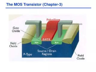
STRUCTURE • All but Fig. 27.1(d) have vertical current flow. • The buried-gate structure is the scheme proposed originally • The planar-gate structure in Fig. 27.1(b) is probably the mist common today. • The critical parameters • The spacing between gates(2a). • The channel doping level(ND).
The doping The depletion regions from the gates do not merge There exists a narrow, neutral channel opening with zero gate bias. Gaps are a few microns, with channel doping levels around the range. The gates are formed by p-n junctions. The SIT operations can be generalized to include metal gates or MIS gates. depletion regions STRUCTURE
CHARACTERISTICS • SIT is a JFET or MESFET • Super-short channel length • Multiple channels connected in parallel • Difference • The gates do not extend close to the source or drain • Punch-through occurs with high drain bias even if the transistor is turned off
CHARACTERISTICS • The depletion regions around the gates do not pinch off the gap • This condition (27.1) • The built-in potential of the p-n junction • (27.2) • A neutral region between the gates with zero gate bias provides a current path for a depletion-mode device • The current conduction is drift in nature and is similar to an FET
CHARACTERISTICS • With negative gate bias • The depletion regions widen • Pinch off the channel • Electrons from the source start to see a potential barrier • This begins when the gate voltage is more negative than • The pinch-off voltage VP is given by (27.3) (27.4)
CHARACTERISTICS • Negative gate voltage raises the barrier • Positive drain voltage lowers the barrier • The efficiency by which the terminal voltages affect the barrier is indicated by (27.5) (27.6)
CHARACTERISTICS • The factors and are geometry dependent • Different for different structures in Fig 27.1 • example (27.7) (27.8)
CHARACTERISTICS • The current of an SIT is given by the form • is the doping concentration is the source • The term is the carrier diffusion velocity • When becomes small giving a current of • The barrier height is given by (27.9) (27.10) (27.11)
CHARACTERISTICS • Diffusion current is exponential with • The current can be put in the form • The I-V characteristics have the form (27.12) (27.13) (27.14) (27.15)
CHARACTERISTICS • Another mode of operation is the bipolar-mode SIT(BSIT) • The gap is smaller • The doping in the channel is lower (27.16) • The output characteristics of a BSIT
APPLICATIONS • Combination of high voltage, high speed capability • Most applications of the SIT are in the power area. • Low noise, low distortion, and low output impedance • It can be used in high-power oscillators of microwave equipment
SIT는높은파워, 높은주파수, 높은온도application을위한short channel FET 구조이다 • SI(Static Induction)소자는 접합게이트에 인가하는 전압에 의해 에미터전류를 제어하는 전압제어형 소자로서, SI Transistor는 수10㎒의 고주파 발진기나 증폭기등에 이용되는 고속용소자인 한편, SI-Thyristor는 고내압용으로 적합하고, GTO보다 고속이며 dv/dt 및 di/dt 내량이 우수하기 때문에 고내압ㆍ고속의 스위치로 인버터 등에 주로 사용되고 있다. • 현재 4㎸/400A의 역도통 SI 싸이리스터가 사용되고 있지만 4.5㎸/1㎄급 용량의 소자의 개발을 목전에 두고 있다. • 이러한 SIT의 특징을 다음과 같이 요약할 수 있다. • - 유니폴라 스위치로써 Tail전류가 작고, 고속 스위칭동작이 가능하다. • - 고내압/대용량의 제품제작이 가능하고, 전력밀도를 높일 수 있다. • - 파워 MOSFET와 비교해서 On저항이 크고 도통손실도 많지만, SIT는 병렬접속이 용이함으로써, 병렬 합성저항을 저하시킬 수 있어 대전류화가 가능하다. • - 파워 MOSFET과 비교해 체널부분의 구조가 단순하므로 전류써지에 강하다. • - 구동ㆍ보호회로가 복잡해진다. • SIT는 이러한 특징에 의해, 정격이 큰 소자는 주파수가 100㎑∼400㎑대의 대전력 인버터에 사용되며, 특히 고주파특성을 개선한 소자는 ㎒대의 고주파 인버터에 사용이 가능하다.