Sequential MOS Logic Circuits
Sequential MOS Logic Circuits. A. Marzuki. Introduction. Sequential Circuit. Behavior of Bistable Elements. SR Latch Circuit. Clocked Latch and Flip Flop Circuits. CMOS D-Latch and Edge-Triggered Flip-Flop. Classification of logic circuits based on temporal behaviour. Sequential circuit.


Sequential MOS Logic Circuits
E N D
Presentation Transcript
Sequential MOS Logic Circuits A. Marzuki
Introduction • Sequential Circuit • Behavior of Bistable Elements • SR Latch Circuit • Clocked Latch and Flip Flop Circuits • CMOS D-Latch and Edge-Triggered Flip-Flop
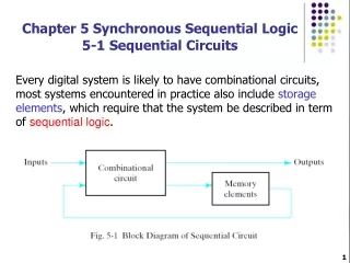
Classification of logic circuits based on temporal behaviour
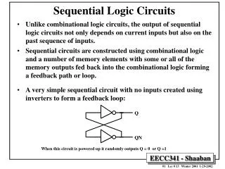
BiStable Voltage gain of inverters is larger than unity at unstable Point, a small voltage perturbation at the input of any of the inverters will be amplified, causing the operation point to move to one of the stable points. simple analogy the energy function P ( x ) could be the potential energy of some one-dimensional mechanical system. The gradient of P ( x ) is a “force”
Bistable At V01 = V02 Unstable condition where gm = (gmN+ gmP) : All four Transistor are in saturation Direction is determined by initial perturbation polarity. Output Expectation (exponential!!!)
Continue… Gate Capacitance >>> Drain Capacitance Gate Charges Derivative of small-signal gate voltages
Continue… Combination above three equations
Continue… Combination of two equation yields 2nd order differential equation Time behaviour of gate charge q1
Continue… Assume ~ Large t
Detailed Truth Table • J, K Compliments Q will go to J value at the next clock edge. J, K HIGH, the output will reverse its state after each clock pulse.
Master-Slave Flip Flop (NOR) • CLK is HIGH MASTER is enable. Slave is disable and retains its previous state. • CLK is LOW is disconnected while input of slaves are simultaneously coupled to the output of the slaves.