solid state electronic materials electronic structure and band energy
390 likes | 863 Vues
solid state electronic materials electronic structure and band energy. to describe electrons and their electrical properties in a solid. qualitative band model. quantitative bond model. Kimia Bahan Semikonduktor – 2010 – Dr. Indriana Kartini. Band Theory of Solids. Energy Levels.

solid state electronic materials electronic structure and band energy
E N D
Presentation Transcript
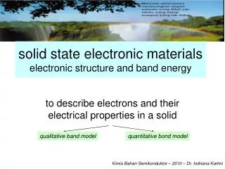
solid state electronic materialselectronic structure and band energy to describe electrons and their electrical properties in a solid qualitative band model quantitative bond model Kimia Bahan Semikonduktor – 2010 – Dr. Indriana Kartini
Energy Levels • Valence band electrons are the furthest from the nucleus and have higher energy levels than electrons in lower orbits. • The region beyond the valence band is called the conduction band. • Electrons in the conduction band are easily made to be free electrons.
Isolated Semiconductor Atoms • Silicon and Germanium are electrically neutral; that is, each has the same number of orbiting electrons as protons. • Both silicon and germanium have four valence band electrons, and so they are referred to as tetravalent atoms. This is an important characteristic of semiconductor atoms.
Semiconductor Crystals • Tetravalent atoms such as silicon, gallium arsenide, and germanium bond together to form a crystal or crystal lattice. • Because of the crystalline structure of semiconductor materials, valence electrons are shared between atoms. • This sharing of valence electrons is called covalent bonding. Covalent bonding makes it more difficult for materials to move their electrons into the conduction band.
2 major binding forces: • Binding forces coming from electron-pair bonds (covalent bonding) • For elemental semiconductors: C(diamond), Si and Ge • typically around 4 eV in semiconductor device • Ionic bonding/heteropolar bonding • For ionic solids such as the nitride, oxide and halide insulators, and compound semiconductors
the motion of electrons (1023) in the solids determines the electrical characteristics of the solid state electronic devices and integrated circuit • in vacuum, the motion of a few separately objects Newton Law; F = ma – classical law of mechanics • for solids there is particle density – classical law must be extended
in a solid high packing density • in a volume of about 1 cm3, there are 1023 electrons and ions packed • in a vacuum tube, there are only 109-1010 electrons • consequences in solids: • very small interparticle distances ((1023)-1/3=2.108 cm) • high interparticle forces (interacting particles) • high interparticle collision (about 1013 per second) • high particle density in solid system condensed matter current or wave generated in solids resulted from averaged motion of electrons statistical mechanics
Kristal fotonik (matriks dan bola mempunyai sifat dielektrik yang berbeda) photons scatter in the periodic lattices non-interacting particles berlaku persamaan Maxwell: solved exactly Band Diagram – standing waves allowed frequencies bands forbidden frequencies band-gaps Kristal (lattice of ions) e- scatter in the periodic lattices interacting particles berlaku persamaan Schrodinger: H = E solved approximately Band Diagram – electron standing waves allowed energies bands forbidden energies band-gaps
quantized energy 1 e- atom discrete energy multielectron system (~ 1023/cm3) Extrapolation on 1 crystal • uncertainties with small distances • large number of particles allowed bands and forbidden bands Wave mechanics applied (Schrodinger eqn.) and statistic mechanics Electronic energy levels are arranged in allowed and forbidden bands results of statistical mechanic analysis at thermodynamic equilibrium give the Fermi-Dirac quantum distribution of the electron kinetic energy in a solid (condensed matter) and Boltzmann classical distribution of electrons and particles in a gas (dilute matter)
1 ELECTRON Math solution to quantum mechanic eqns model 1 electron energy level of 1 electron ELECTRONIC SOLIDS • Applied : • Planck eqn. (EMR energy and quantized particle wave) • E = h • de Broglie eqn. (EMR momentum and particle wave ~ 1/) • p = h/ energy level of 1 electron band energy
Bands formation As the two atoms interact overlap the two e- interact interaction/perturbation in the discrete quantized energy level splitting into two discrete energy levels
allowed band • at r0 : allowed band consists of some discrete energy level • Eg.: System co. 1019 atoms 1e, the width of allowed band energy at r0 = 1 eV • if assumed that each e- occupies different energy level and discrete energy level equidistance allowed bands will be separated by 10-19 eV r0 represents the equilibrium interatomic distance in the crystal • The difference of 10-19 eV too small allowed bands to be quasi-continueenergy distribution
Bands of atom 3e- As 2 atoms get closer, electron interaction was started from valence electron, n=3 pita energi terbolehkan pita energi terlarang At r0 : 3 allowed bands separated by forbidden were formed
Splitting energi pada atom 14Si 4 elektron valensi 3s2 3p2 Eg represents the width of forbidden band = bandgap energy 3p2 : n=3 l=1 3s2 : n=3 l=0 At reduced distance : 3s and 3p interacted dan overlap 4 quantum state of upper bands (CB) and 4 quantum state of lower bands (VB) 4 valence e- of Si will occupy lower band
Bonding In Metals: Lithiumaccording to Molecular Orbital Theory
Sodium According to Band Theory Conduction band: empty 3s antibonding No gap Valence band: full 3s bonding
Magnesium 3s bonding and antibonding should be full
Magnesium Conduction band: empty No gap: conductor Valence band: full Conductor
Classification of solids into three types, according to their band structure • insulators: gap = forbidden region between highest filled band (valence band) and lowest empty or partly filled band (conduction band) is very wide, about 3 to 6 eV; • semiconductors: gap is small - about 0.1 to 1 eV; • conductors: valence band only partially filled, or (if it is filled), the next allowed empty band overlaps with it
Band gaps of some common semiconductors relative to the optical spectrum Visible Ultraviolet Infrared GaAs TiO2 GaP Ge Si CdSe CdS SiC ZnS InSb Eg (eV) 0 1 2 3 4 (m) 7 5 3 2 1 0,5 0,35
Energy band gap • determines among other things the wavelengths of light that can be absorbed or emitted by the semiconductors • Eg GaAs = 1.43 eV corresponds to light wavelengths in the near infrared (0.87 m) • Eg GaP = 2.3 eV green portion of the spectrum • The wide variety of semiconductors band gap tunable wavelength electronic devices • broad range of the IR and visible lights LEDs and lasers
Electron Distribution • Considering the distribution of electrons at two temperatures: • Absolute zero - atoms at their lowest energy level. • Room temperature - valence electrons have absorbed enough energy to move into the conduction band. • Atoms with broken covalent bonds (missing an electron) have a hole present where the electron was. For every electron in the conduction band, there is a hole in the valence band. They are called electron-hole pairs (EPHs). • As more energy is applied to a semiconductor, more electrons will move into the conduction band and current will flow more easily through the material. • Therefore, the resistance of intrinsic semiconductor materials decreases with increasing temperature. • This is a negative temperature coefficient.
If the temperature increases, the valence electrons will gain some thermal energy, and breaks free from the covalent bond → It leaves a positively charged hole. In order to break from the covalent bond, a valence electron must gain a minimun energy Eg: Bandgap energy At 0°K, each electron is in its lowest possible energy state, and each covalent bounding position is filled. If a small electric field is applied, the electrons will not move → silicon is an insulator
Compound Semiconductor: combination of elements • For elemental/intrinsic semiconductor of Si and Ge: the filled valence band of 4 + 4 = 8 electrons • For non-intrinsic semiconductor: the filled valence band of 8 electrons constructed by combination of elements of group II-VI and III-V • the E for the bandgap will differ from the elemental semiconductors • the bandgap will increase as the tendency for the e- to become more localised in atom increases (a function of constituent electronegativities)
Impurities • strongly affects the electronic and optical properties of semiconductor materials • used to vary conductivities from apoor conductor into a good conductor of electric current • may be added in precisely controlled amounts doping Evaluation of both properties needs prior understanding of the atomic arrangement of atoms in the materials – various solids
Empirical relationship between energy gap and electronegativities of the elements Metallic conductance (Sn) Elemental semiconductors (Si, Ge, etc) Compound semiconductors (GaAs, CdS, etc.) • Insulators: • Elemental (diamond, C) • Compound (NaCl)
Impurity and Defect Semiconductor: Creating band gap through electronegativity effect P-type n-type
Semiconductor Doping • Impurities are added to intrinsic semiconductor materials to improve the electrical properties of the material. • This process is referred to as doping and the resulting material is called extrinsic semiconductor. • There are two major classifications of doping materials. • Trivalent - aluminum, gallium, boron • Pentavalent - antimony, arsenic, phosphorous
Energy bandmodel and chemical bondmodel of dopants in semiconductors (a) donation of electrons from donor level to conduction band; (b) acceptance of valence band electrons by an acceptor level, and the resulting creation of holes; (c) donor and acceptor atoms in the covalent bonding model of a Si crystal.
