Memory and Programmable Logic
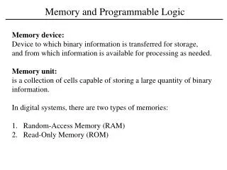
Memory and Programmable Logic. Memory device: Device to which binary information is transferred for storage, and from which information is available for processing as needed. Memory unit: is a collection of cells capable of storing a large quantity of binary information.

Memory and Programmable Logic
E N D
Presentation Transcript
Memory and Programmable Logic • Memory device: • Device to which binary information is transferred for storage, • and from which information is available for processing as needed. • Memory unit: • is a collection of cells capable of storing a large quantity of binary • information. • In digital systems, there are two types of memories: • Random-Access Memory (RAM) • Read-Only Memory (ROM)
Memory and Programmable Logic • 1.Random-Access Memory (RAM): • The process of transferring new information into memory is the • memory write operation. • The process of transferring information out of memory is the • memory read operation. • 2.Read-Only Memory (ROM): is an example of programmable logic • device (PLD). Other examples are: programmable logic array (PLA), • programmable array logic (PAL), and field-programmable logic gate • array (FPGA). (PAL: Program. AND, fixed OR, PLA: Program. AND/OR) • A PLA is an integrated circuit with internal logic gates that are • connected through electronic paths, which behave similar to fuses. • Programming the device involves blowing those fuses along the • paths that must be removed to obtain a desired function.
Random-Access Memory Memory unit stores binary information in groups of bits called words. Memory word group of 1’s and 0’s and may represent a number, character(s), instruction, or other binary-coded information. Most computer memories use words that are multiples of 8 bits (byte). 32-bit word 4 bytes
Random-Access Memory Each word in memory is assigned an address 0 up to 2k – 1 (k = # of address lines). memory content
RAM: Write and Read Operations To transfer a new word to be stored into memory: 1. Apply the binary address of the word to address lines. 2. Apply the data bits that must be stored in memory to the data input lines. 3. Activate the write input. To transfer a stored word out of memory: 1. Apply the binary address of the word to address lines. 2. Activate the read input.
Write and Read Operations in RAM The memory enable switches to the high level and the Read/Write to the low level. The two control signals must be active for at least 50 ns. The memory enable switches to the high level and the Read/Write to the high level. The memory places the data of the word selected by the address in to the output data lines 50 ns from the time the memory enable is activated.
Memory Types • Integrated circuit RAM units are available in two possible operating modes: • static and dynamic. • Static RAM (SRAM) consists of of internal latches that store the binary • information. The stored information remains valid as long as power is • applied to the unit. • Dynamic RAM (DRAM) stores the binary information in the form of • electric charges on capacitors provided by the MOS transistors. • The charge on the capacitors tends to decay with time and the capacitors • must be periodically recharged by refreshing of the dynamic memory every • few milliseconds. • DRAM offers reduced power consumption, large integration of units on chip. • SRAM is easier to use and has shorter read and write cycles.
Volatile vs. Non-Volatile Memory • RAM (static and dynamic) is said to be volatile, since information is lost when power is turned off. • Non-volatile memory retains its information even when power is turned off. • Magnetic disks: stored data is represented by the direction of magnetization. • CD: compact disc is a piece of polycarbonate (a type of plastic) on which a spiral track has been impressed. This spiral track is a series of indentations ("pits") separated by flat areas ("land"). • ROM: The internal storage elements are set to their values once and after that are only read.
EPROMS and PROMS Erasable Programmable Read-Only Memory (EPROM) is a special type of memory that retains its contents until it is exposed to ultraviolet light. To write to and erase an EPROM, you need a special device called a PROM ProgrammerorPROM burner. An EPROM differs from a PROM in that a PROM can be written to only once and cannot be erased. EPROMs are widely used in personal computers since they enable the manufacturer to change the contents of the PROM before thecomputer is actually shipped. This means that bugs can be removed and new versions installed shortly before delivery. Electrically Erasable Programmable Read-Only Memory (EEPROM), is like EPROM except that the previously programmed connections can be erased with an electrical signal.
Memory Cell The storage part of the cell is modeled by an SR latch with associated gates. A = 1 in the read/write input provides the read operation by forming a path from the latch to the output. A = 0 in the read/write input provides the write operation by forming a path from the input to latch.
4 x 4 RAM When memory select = 1 one of the four words is selected. READ Operation: the four bits of the selected word go through OR gates to the output terminals. WRITE operation: the data available in the input lines are transferred into the four binary cells of the selected word. The memory cells that are not selected are disabled.
RAM Commercial RAM thousands of words, with each word 1 - 64 bits. A memory with 2k words of n bits/word requires k address lines that go into a kx 2k decoder.
Two Dimensional Decoding 404 The idea of two-dimensional decoding is to arrange the memory cells in an array that is close an possible to square. Use two k/2-input decoders instead of one k-input decoder. One decoder performs the row selection and the other the column selection in a two dimensional matrix configuration. Q: How many words can be selected?
Read-Only Memory (ROM) Read-only memory is a memory device in which permanent binary information is stored. • The number of words in a ROM is determined from the k address • input lines needed to specify the 2k words. • The ROM does not have data inputs because it does not have the • write operation.
Read-Only Memory (ROM) A 32 x 8 ROM consists of 32 words of 8 bits each. The five input lines are decoded by into 32 distinct outputs (memory addresses) using a 25x 8 decoder. Each OR gate has 32 input connections 32 x 8 ROM has internal connections 32 x 8. In general, a 2kxn ROM will have k x 2k decoder and n OR gates with 2kxn internal connections.
Programming the Read-Only Memory crosspoint 256 programmable intersections A programmable connection (a crosspoint) between two lines is logically equivalent to a switch that can be be closed (two lines are connected) or open (two lines are disconnected). A switch can be a fuse that normally connects the two points, but can be opened by blowing the fuse using a high voltage pulse.
Programming the Read-Only Memory 1 address 3 1 memory content 1 1 0 1 0 1 0 0 0 0 0 Output A6 can be expressed in sum of minterms as:
Programmable Logic Device (PLD) product terms for Boolean functions sum terms for Boolean functions
Programmable Logic ARRAY (PLA) crosspoint ‘connected’ crosspoint ‘disconnected’
PLA Programming Table Inputs Outputs A B C F1F2 product term • 0 - 1 - • 1 - 1 1 1 • 1 1 - 1 • 0 1 0 1 - Path between inputs and AND gates = inputs in programming table 1 connection from input variable to AND gate 0 connection from the complement of input variable to AND gate - blown fuse in the input variable and in its complement Path between AND and OR gates = outputs in programming table 1 connection from output of AND gate to OR gate - blown fuse.
PLA Programming example Implement the following function with a PLA:
Programmable Array Logic (PAL) The programmable array logic (PAL) is a logic device with fixed OR array and a programmable AND array. It is user ‘friendly PAL’: easier to program but not as flexible as PLA. Boolean functions must be simplified to fit into each section product term cannot be shared among two or more gates. Outputs Inputs programmable input
Sequential Programmable Logic Devices • 1. Simple or Sequential Programmable Logic Device (SPLD): • Includes flip-flops and AND-OR array within the IC chip.
Sequential Programmable Logic A microcell is a section of a SPLD that contains a sum-of-product combinational logic and an optional flip-flop. A commercial SPLD contains 8 - 10 microcells in an IC package.
Complex Programmable Logic Device (CPLD) 2. Complex Programmable Logic Device (CPLD): The design of a complete digital system using PLD requires the use of several PLD’s in a Complex Programmable Logic Device (CPLD) integrated on a singlechip. I/O block provides the interconnections to the IC pins switch matrix received inputs from I/O and directs them to the individual microcells.
Field-Programmable Gate Array (FPGA) • 3. Field-Programmable Gate Array (FPGA): is a VLSI circuit whose • function is defined by a user's program rather than by the manufacturer • of the device. • Depending on the particular device, the program is either 'burned' in • permanently or semi-permanently as part of a board assembly process, • or is loaded from an external memory each time the device is powered up. • The Field-Programmable Gate Arrays provide the benefits of custom • CMOS VLSI, while avoiding the initial cost and time delay.

