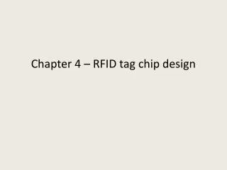
Comprehensive Overview of RFID Tag Chip Design and Circuit Architectures
250 likes | 365 Vues
This chapter delves into the intricacies of RFID tag chip design, including system architecture and the Gen2 protocol's frame-sync sequence. It highlights power generation through multi-level voltage systems and elucidates N-stage Dickson charge pumps. Key factors affecting power conversion efficiency are discussed alongside variations of charge pump circuits featuring self-threshold and dynamic compensation. The chapter also presents innovative CMOS architectures, sense amplifiers, and energy-efficient adiabatic circuits, along with practical examples and schematic representations.

Comprehensive Overview of RFID Tag Chip Design and Circuit Architectures
E N D
Presentation Transcript
Figure 4.5 The factors affecting the power conversion efficiency of the charge pump
Figure 4.6 Charge pump circuit with self-threshold compensation
Figure 4.7 Charge pump circuit with constant threshold compensation and substrate shift
Figure 4.8 Symmetrical charge pump circuit with dynamic threshold compensation
Figure 4.12 Schematic (a) control capacitor Mc and tunneling capacitor Mt (b) cross section
Figure 4.14 (a)Voltage-mode sense amplifier (b) Current-mode sense amplifier
Figure 4.16 Decode Margin for 1.28 MHz with 5% clock uncertainty (violations marked with the circle)
Figure 4.17 Decode Margin for 1.92 MHz with 5% clock uncertainty
Figure 4.18 BLF error when clock rate is 1.28 MHz (violations marked with the circle)
Figure 4.21 Example of adiabatic CMOS circuit (left) versus standard CMOS Logic (right)
Figure 4.23 The different package of on-chip antenna and tag chip