Download
1 / 24
240 likes | 345 Vues
This presentation outlines the design of a cutting-edge direct sampling receiver for 2-GHz radios. With a focus on circuit design, loop filters, PLL, and measurement results, the system achieves exceptional SNR performance and noise floor across a 60-MHz bandwidth. The use of advanced components like MOS-HBT cascodes and high-speed DACs ensures superior linearity and noise characteristics, enabling a groundbreaking 9.65-bit resolution. The presentation also highlights the impact of clock jitter, PLL performance, and system-level design considerations. Acknowledgments include funding support from Nortel Networks and collaboration with industry partners for chip fabrication and testing.

E N D
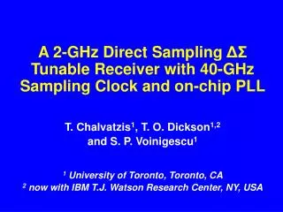
A 2-GHz Direct Sampling ΔΣ Tunable Receiver with 40-GHz Sampling Clock and on-chip PLL T. Chalvatzis1, T. O. Dickson1,2 and S. P. Voinigescu1 1 University of Toronto, Toronto, CA 2 now with IBM T.J. Watson Research Center, NY, USA
Outline of Presentation • Motivation • Circuit design • Loop filter • PLL • Measurement results • Summary
Motivation • Direct sampling receiver for 2-GHz radio with 60 MHz BW • CT BP ΔΣ ADC with SNDR of 55dB/60MHz [Chalvatzis et al., JSSC, May 2007] • Investigation of clock jitter impact with on-chip clock source
System Architecture • 2-GHz Gm-LC BPF • Fourth order loop • 1-bit quantizer as DFF with FCLK=40GHz • RZ pulse DACs • 40-GHz VCO/PLL
System Level Design • Design methodology in continuous-time • System level simulation for accurate analysis of loop delay • Loop coefficients: • Gm1=22mS, Gm2=15mS • Gfb1=50mS, Gfb2=150mS SNDR=61dB over 60 MHz in Matlab Simulink
SNR vs clock jitter • Clock jitter effect simulated for FS=40GHz, OSR=333 • PLL jitter < 1.4 ps (rms) for 10 bits resolution Δ: quantizer step [Ortmanns et al., ISCAS 2003]
SNR vs resonator Q • Quantization noise integrated over BW for FS=40GHz • Q >18 for 10 bits resolution
Loop Filter • MOS-HBT cascode for high linearity and low noise • EF limit voltage headroom, current source adds noise Loop filter with EF
Modified Loop Filter • MOS-HBT cascode for high linearity and low noise • EF limit voltage headroom, current source adds noise Modified Loop Filter
D/A Converter – Quantizer • DAC and quantizer with MOS-HBT cascodes [Chalvatzis et al., JSSC, May 2007] • MOS on clock path to improve speed with low supply • HBT on data path for high gain DAC Latch
Digital Receiver – PLL Blocks • 40-GHz PLL design from 2.5V challenging • Combination of MOS-HBT transistors in PLL blocks Resettable Latch
Digital Receiver – PLL Blocks • 40-GHz PLL design from 2.5V challenging • Combination of MOS-HBT transistors in PLL blocks Charge Pump
VCO • Colpitts VCO topology with HBT [Dickson et al., CSICS 2006] • VCO biased for minimum phase noise • Differential tuning with accumulation mode MOS varactors
ADC DIGITAL OUT RF IN PLL REF PLL SEL Fabrication • ADC with on chip VCO/PLL in STM 0.13μm SiGe BiCMOS • Power dissipation 2.19W from 2.5V • Chip size 1.59x2.39mm2
PLL measurements • Phase noise/jitter measured on PLL test structure • RMS jitter: σt=849fs • Jitter limited SNR for Fo=2GHz and OSR=333 -> SNR=66.7dB
VCO measurements • Phase noise < -103dBc/Hz at 1 MHz offset from 40-GHz carrier
Spectrum measurement with PLL • ADC tested with external and on-chip clock • No significant degradation from on-chip clock • Feedthrough from 2.5GHz PLL reference does not degrade performance
SFDR measurement SFDR=59dB
SNDR measurement SNDR measured for FIN=2GHz, FS=40GHz SNDR = 59.8dB over 60 MHz
Dynamic Range ADC noise floor the same (-65dBm/60MHz) when external and on-chip clock employed
Conclusion • First mm-wave sampling ΔΣ digital receiver in any semiconductor technology • Digital receiver achieves 9.65-bit resolution over 60 MHz • Removing EF pair in filter helps to increase linearity of ADC loop filter • For 10-bits resolution, jitter from on-chip VCO/PLL not limiting performance • Noise floor set by resonator Q
Acknowledgements • Nortel Networks for funding support • John Ilowski and Eric Gagnon for discussions • STMicroelectronics for chip fabrication • Prof Miles Copeland for advice on the manuscript • Ricardo Aroca for help with testing • CMC for CAD tools • Jaro Pristrupa for CAD support