Field Effect Transistors using Carbon Nanotubes
350 likes | 382 Vues
Explore the world of carbon nanotube FETs. Learn about their high sensitivity, fabrication techniques, and applications as biosensors and chemical sensors. Dive into how NTFETs work, detection capabilities, and film deposition methods for improved performance.

Field Effect Transistors using Carbon Nanotubes
E N D
Presentation Transcript
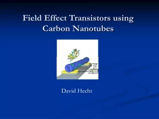
Biosensor Field Effect Transistors using Carbon Nanotubes David Hecht
Why Study NTFET’s? Bacteria 1 m 100 nm Virus Proteins 10 nm Biosensor 1 nm DNA 0.1 nm • Size!!! • Diameter ≈ 1nm, length ≈ 1 micron • Quasi 1-D object • High Mobility Semiconductors • Moore’s Law • Can be p-type or n-type • Flexible Transistors/Electronics? • Sensor • Biosensor (walls can be functionalized) • Chemical Sensor • high sensitivity/large surface area
How a NTFET Works p-type in air Source Drain Insulating Layer (SiO2) Conducting “Gate” (p type Si) Rprot VRprot Isd Vgate Vsd Vg = 0
How a NTFET Works p-type in air S D Insulating Layer (SiO2) Conducting “Gate” (p type Si) Rprot VRprot Isd Vg Vsd Vg = positive, Holes are Depleted
How a NTFET Works p-type in air S D Insulating Layer (SiO2) Conducting “Gate” (p type Si) Rprot VRprot Isd Vg Vsd Vg = negative, Holes are enhanced
Nanotube FET transistor S D SiO2 AFM image Si back gate Vsd Vg Isd Ideal NTFET Device A A. Max Conductance B. Modulation – Signal to Noise C. Transconductance (slope at zero gate) Mobility of Carriers (electrons or holes) D. Threshold Shift – Changes in Doping p-type C Conductance (S) B D Gate Voltage (V)
Effect of charge transfer on the device electronics Detection of gases1 NH3 el. donor NO2 el. acceptor 1Bradley, K.; Gabriel, J.-C. P.; Briman, M.; Star, A.; Grüner, G. “Charge Transfer from Ammonia Physisorbed on Nanotubes,” Phys. Rev. Lett.2003, 91, 218301.
Single Nanotube vs. Network Novel active electronic devices • Single tube/fiber channel • greater sensitivity • individual device fabrication (basic research) • Network channel • easier/more consistent device fabrication • Applications
Metallic vs. Semiconducting Determines geometry and diameter Armchair: (n, n) Zig-Zag: (n, 0) If n – m is a multiple of 3, the nanotube is metallic. 1/3 of NT’s are metallic,2/3 are semi-conducting!!!!
On/Off Ratio Low Lots of Metallic Tubes Metallic Tubes are the Enemy ISD ISD On/Off Ratio High VG VG Vg Few Metallic Tubes D NT Film V Metallic Tubes Act To Screen Potential from outermost tubes of Film!!! x Si gate SiO2 S
Deposition Techniques Want: Uniform Film of individually separated NT’s • Direct Deposition • Drop Casting -- Flocculation due to Van der Waals between tubes limits uniformity. • Spin Coating – work in progress • Langmuir-Blodgett/Quasi-Langmuir-Blodgett • Separate Tubes using Solubilization Agents • Starch/Enzymes • PmPV
Quasi-Langmuir-Blodgett Film • DEPOSITION METHOD • 1. Dissolve NT’s in Solvent by Sonication. Single tube dissolution is ideal. For a solvent we used a 10:1 mixture of ortho-xylene and 1,2-dichlorobenzene.
Alumina Filter (pore size = 20nm)* Quasi-Langmuir-Blodgett Film • DEPOSITION METHOD • 2. Quickly suck fluid through a porous alumina filter (pore size = 20 nm) * From Whatman website
Quasi-Langmuir-Blodgett Film • DEPOSITION METHOD • 3. While film is still slightly damp with solvent, wash water over filter. Film will break off as a “raft” and float to top.
Substrate Quasi-Langmuir-Blodgett Film DEPOSITION METHOD 4. Put in substrate and suck out water to redeposit the film.
Why 10:1 solvent mixture? • Ortho-xylene:Dichlorobenzene solvent mixture used for 3 reasons • 1) High nanotube solubility ≈ 15 mg/L • 2) Specific Gravity < 1 (so rafts can float) • 3) Immiscibile in water
Film on Glass Slide Quasi-Langmuir-Blodgett Film ADVANTAGES DISADVANTAGE • Film fairly uniform over large area • Thickness of Film controllable. (20nm-1um) • Room Temperature Technique vs. CVD at 900o C • Film’s too thick. Can’t get monolayer.
200 nm SEM of Nanotube Film1 Does water Immersion affect Films? Temperature Dependence of Resistivity1 • MECHANICAL • Film consists of well separated ropes of ≈10 nm before and after immersion • ELECTRICAL • Immersion in water does not affect DC resistivity. 1N. Peter Armitage
Quasi-LB Film: Are They Uniform? 30 nm thick film 80 nm thick film 50 microns Average “roughness” = 36 nm Average “roughness” = 14 nm “Roughness” = Σ|(xi - xave)|/n *Data taken in UCLA Nanolab using Nano-Or 3-D Scope 2000 for 2D profiles, and Dektak 8 profiler to measure film thickness
SiO2 Device Fabrication • Steps to making Device • 5000 Ao SiO2 on doped Silicon • commercially bought, HF remove SiO2 from one side • Deposit NT Film • Evaporate Gold source and drain through shadow masking • Use Silver epoxy to attach wires • Clamp onto metal chuck to apply Vg • Dielectric BreakdownBreakdown Electric Field in SiO2 = 1 x 10⁷ V/cm
Measurement Setup p-type in air S D • Output (Vg ) ±100 V quasi-AC Sawtooth Waveform. • Output bias voltage (100mV) across SD, and measure Isd • Measure Voltage across Rprot to get Ileakage SiO2 p type Si back gate 200 V VRprot Rprot Isd Vg Vsd
Transistor Characteristics Film = 4000 Angstroms thick (≈400 NT layers) => 2% Modulation!!
Transistor Characteristics Vg = 0 Vg = 50 Vg = 100 Blew on Sample Notice the slow drift…Need to stabilize temperature for future measurements
Transistor Characteristics Film = 800 Angstroms thick (≈80 NT layers) => 20% Modulation!!
Transistor Characteristics Film = 300 Angstroms thick (≈30 NT layers) => 40% Modulation!!
Calculation of Mobility • Quadratic Model of MOSFET: • ISD = (μCoxW)[(VGS – VT)VDS – VDS2/2] for VDS << VGS – VT • Slope of IVg curve = μCoxWVDS Plugging in the numbers yields mobility of 0.9 cm2/V*s Mobility's: Single Carbon NT = 105 Silicon = 102-103 NT Network = 101 Organic Semiconductor = 10-4 - 10-1 High Mobility means device can operate at Higher frequency!!! L L
Liquid Gating 50 % Modulation!! AluminaFilter on glass Liquid Gating Setup Data for 1000 Angstrom thick sample1 • Larger Modulation than Bottom Gating => liquid penetrates porous film • Liquid Gating useful for protein/biomolecule detection. 1Data taken with aid of Mikhail Briman
Nanotube Reflux in Nitric Acid O Original Nanotube H After 20 Hour Reflux in HNO3 O Carboxylic Acid Group OH O After filtering and rinsing in water At PH 7 Becomes Polar O -
Did Refluxing Work? 1 Minute after Sonication 10 Minute after Sonication
Did the Reflux Work? 24 Hours after Sonication
Future Work • Improve Device Characteristics • Thinner Films • More Dispersed Tubes • Separate Semiconducting and Metallic Tubes • Mobility vs. applied pressure • Improve Probe Station • True AC Setup • Gold Pogo Pin probe/Micrometer positioner • Temperature/Humidity Control Chamber • Characteristics vs. Network Density • Photo-lithographic Mask for micro scale geometries • Study 2-D Percolation problem of random array of semiconducting rods • E-Beam Lithography for nano scale geometries • Protein detection
Conclusion • Created NT network transistor using room temperature fabrication process • Film too thick to get good characteristics.
Thanks • The Gruner Group: Peter Armitage, M. Briman, Erika Artukovic, Liangbing Hu, George Gruner • The Chemists: Erik Richman, Will Molenkamp (Tolbert); Matt Spotnitz (Kaner). • Steve Franz (Nanolab). • MCTP
