Download
1 / 26
650 likes | 1.97k Vues
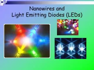
Nanowires and Light Emitting Diodes (LEDs). Nanowires. What Is A Nanowire? Any solid material in the form of wire with diameter smaller than about 100 nm. Transmission electron micrograph of an InP/InAs nanowire. E. ε 13. ε 12. ε 11. 0. k x. Nanowire quantization.

E N D
Nanowires What Is A Nanowire? Any solid material in the form of wire with diameter smaller than about 100 nm. Transmission electron micrograph of an InP/InAs nanowire
E ε13 ε12 ε11 0 kx Nanowire quantization Confinement of a particle in two directions leads to additional energy quantization and leaves only one degree of freedom. Scanning electronic microscope image of free-standing InP quantum wires (from Thomas Mårtensson, Patrick Carlberg, Magnus Borgstrom, Lars Montelius, Werner Seifert, and Lars Samuelson, Nano Letters, Vol. 4, No. 4, pp. 699-702 (2004 ) ). Adapted from lecture summary #06 from Dr. Mitin’s EE240 Lecture
How are they Made? • The Scanning Tunneling Microscope (STM) can be used to image surfaces or to manipulate atoms. • Nanowires can be made by crashing the tip of an STM into a substrate and then retracting. A bias voltage can be applied between the tip and sample allowing current and resistance measurements. • The STM can also be used to locally oxidize a pattern onto thin films of Si which in return is used to pattern nanometer sized wires single rows of Indium atoms on a Silicon surface. The picture was taken with a Scanning Tunneling Microscope
schematic of the process used to fabricate the wires Nanowires can also be made using lithography techniques. The advantage to this method is that many wires can be made at once. Wires of 50nm width have been fabricated.
Another method of fabrication is the capillarity-induced filling of carbon nanotubes. Many materials have been used to fill the carbon nanotubes such as Pb, Ni, Cr, Ge, S, Dy, etc. The picture above shows an example. One can see the concentric carbon nanotubes encapsulating the PbO center. Nanoporous templates Electron deposition
Growing Nanowires • Put iron nanopowder crystals on a silicon surface • Put in a chamber • Add natural gas with carbon (vapor deposition) • Carbon reacts with iron and forms a precipitate of carbon that grows up and out • self-assembly is the most important fabrication technique, because of the large number of structures you can create quickly http://www.rpi.edu/dept/materials/COURSES/NANO/bartolucci/index.html
Diodes • Current flows in only one direction • P-N Junction and Depletion Region • Forward bias, Reverse bias
Reverse Bias Forward Bias • Reverse bias prevents current from flowing • Forward bias gives electrons additional energy to overcome depletion region barrier
Light Emission • Electron recombines with hole under forward bias, Photon of light is emitted with characteristic frequency • E = hw (eV) , frequency emitted is proportional to the voltage applied multiplied by the elementary charge • Electrons and holes combine radiatively (with a photon) or nonradiatively (with a phonon) in the depletion region E2 E1 ħω = E2 – E1 Adapted from lecture summary #20_1 from Dr. Mitin’s EE240 Lecture
Electron recombination in direct bandgap semiconductors emits photons (light) • Recombination in indirect bandgap emits phonons to allow for momentum conservation Adapted from lecture summary #08 from Dr. Mitin’s EE240 Lecture
Radiative Recombination Rates • Rate of recombination is proportional to both the electron and hole concentrations • Spontaneous Recombination vs Hole Concentration with multiple models
Non-Radiative (Phonon) Recombination Rates • “Deep Levels” (Shockley-Read Equation) • Auger Recombination • Surface Recombination
Optical Properties, Efficiency, and Temperature • Not all light emitted escapes semiconductor Reabsorption and Extraction Efficiency material Fraction of light that escapes = (1/2) (1-cosφc) Fraction can be increased by a factor of 2-3 by encapsulation
Types of LED Materials • Aluminum Gallium Arsenide (AlGaAs) - red and infrared • Aluminum Gallium Phosphide (AlGaP) – green • Gallium Arsenide Phosphide (GaAsP) - red, orange-red, orange, and yellow • Gallium Nitride (GaN) - green, pure green (or emerald green), and blue • Indium Gallium Nitride (InGaN) - near ultraviolet, bluish-green and blue • Silicon carbide (SiC) as substrate – blue • Zinc Selenide (ZnSe) – blue • Diamond (C) - ultraviolet
Zinc Oxide • Zinc Oxide (ZnO) Research • P-type ZnO nanowires were once difficult to synthesize • ZnO emits high quality light • Efficient for imaging, data storage and biological/chemical sensing • Much lower manufacturing cost then Gallium Nitride (GaN) LEDs GaN Nanowires ZnO Nanowire
Traditional Lighting (Incandescent Bulbs) • Tungsten Filament heats up as current passes through it • Atoms vibrate, electrons are temporarily boosted to higher energy levels • Drop of electrons from higher levels to lower ones creates light • Advantages: Cheap to produce, automatically create white light • Disadvantages: High percentage of energy going towards heat, not as durable or as long lasting as LED’s
Voltage difference across tube causes electrons to flow Mercury atoms are converted from liquid to gas state Electrons collide with gaseous mercury atoms, exciting them to a higher energy state and releasing light Majority of the light is ultraviolet; phosphor coating of tube converts this ultraviolet light into visible white light Advantages: More efficient than traditional lighting, longer lifespan Disadvantages: Operating temperature, “flicker” at twice the operating frequency, safe disposal of mercury Fluorescent Lamps
LEDs • Positive voltage is applied across the pins to excite electrons/holes in the diode • Electrons that jump energy levels emit light of ONE specific energy (and frequency) • LED housing designed to reflect as much of this light forward as possible • Can be much more efficient than both incandescent and fluorescent lighting
Efficiency • LEDs shipping from manufacturers in 2006 are approaching the efficiency of compact fluorescents (CFs) • Standard CF’s – 60 lumens/watt • LEDs – 50-60 lumens/watt • Compare to Standard 100 watt incandescent • 17 lumens/watt • LED’s projected to reach 150 lumens/watt within 10 years
Flexible • Organic LEDs (OLEDs) are lighter and flexible. Some possible future applications of OLEDs • Inexpensive, flexible (rollable) displays • Wall decorations • Night vision (cheaper) • Luminous cloth or clothing • Imagine a screen on your jacket arm.
(Not So) Future Applications of OLEDs Flexible computer and media screens. Can be easily rolled up for convenient storage. OLEDs can be woven, or possibly sprayed, onto articles of clothing. Allows people to bring their media wherever they go.
DieMount Spotlight LEDs • With traditional LEDs valuable light loss occurs • LEDs design allows almost all the light to be captured • Light is projected at a solid angle of +/- 3-4° • Low operating current • Longer lasting, lower power consumption • Applications
Water Treatment • Ultraviolet (UV) radiation causes damage to the genetic structure of bacteria making them incapable of reproduction. • Reduce bacteria levels in flowing raw sewage by 60% using ultraviolet LEDs • Hydro-Photon’s chamber reduces the level of e-coli in contaminated water • Reduces e-coli by 99.99% flowing at 300 ml/minute • These rates are close to values required for individual water treatment systems
References • Tom Harris. "How Light Emitting Diodes Work". January 31, 2002 <http://www.howstuffworks.com/led.htm> (April 26, 2007) • Craig Freudenrich, Ph.D.. "How Light Works". July 10, 2000 <http://www.howstuffworks.com/light.htm> (April 26, 2007) • Schubert, E. Fred. Light-Emitting Diodes. 2nd. Cambridge: Cambridge University Press, 2006. • Gavryushin, V. "The Diode." Functional Combinations in Solid States. 06 June 2006. 26 Apr 2007 <http://www.mtmi.vu.lt/pfk/funkc_dariniai/diod/index.html.> • Frensley, William R. " Heterostructure and Quantum Well Physics." 21 May 1995. University of Leeds. 26 Apr 2007 <http://www.utdallas.edu/~frensley/technical/hetphys/node1.html>. • "Nanowire Research, LED Breakthrough." TechNews. 03 Jan 2007. 26 Apr 2007 <http://www.technologynewsdaily.com/node/5579>. • Narayan, A L. "ZnO nanowires promise more efficient LEDs." Optics.org. 17 Jan 2007. 26 Apr 2007 <http://optics.org/cws/article/research/26830>. • Hogan, Hank. "A Single Dot Marks the Spot for Nanowire LEDs." Photonics Spectra. April 2007. Laurin Publishing. 26 Apr 2007. <http://www.photonics.com/content/spectra/2007/April/LED/87162.aspx>. • "LED basic knowledge." LED Professional. 26 Apr 2007 <http://www.ledprofessional.com/content/view/241/78/#1.2%20Blue%20and%20white%20 LEDs>. • Wyckoff, Susan. "What is a Light-Emitting Diode?." Experiments By Exploration. 1997. Department of Physics and Astronomy, Arizona State University. 26 Apr 2007 <http://acept.la.asu.edu/courses/phs110/expmts/exp13a.html>. • Bai, Yuan Qiang Bai, Ying Dai, Zhong Lin Wang, Yue Zhang. “Bicrystalline zinc oxides nanowires. Chemical Physics Letters. 9 May 2003 • Atwee, Tarek, Sandra Borner, Andreas Pohlkotter, Wolfgang Schade. “Zinc oxide nanowires.” TU Clausthal: LaserAnwendungsCentrum. 26 Apr 2007. <http://lac.tu-clausthal.de/foreschung/zinc-oxide/nanowires/> • “Organic LED Displays (OLEDS). 26 Apr 2007. <http://www.ideasstorming.tw/blog/domotoro7176/idea840> • Patch, Kimberly. “Crossed nanowires make Lilliputian LEDs.” TRN: The Latest Technology Research News. 17 Jan 2001. 26 Apr 2007. <http://www.trnmag.com/Stories/011701/Crossed_nanowires _make_Lilliputian_LEDs_TRN_0011701> • Savage, Neil. “Efficiency Jump for White OLEDs.” Technology Review. 20 Nov 2006. 26 Apr 2007. <http://www.technologyreviews.com/Printer_friendly_article.aspx?id=17808> • “Cheaper LEDs from Breakthrough in Zinc Oxide (ZBO) Nanowire Research, Nano Letters Study Says.” NanoTechwire,com. 6 Jan 2007. 26 Apr 2007. <http://www.nanotechwire.com/news.asp?nid=4187&ntid=115&pg=1> • “Spotlight LED.” 29 March 2007. 26 Apr 2007. <http://optics.org/cws/product/P000002170> • Garfinkel, Simson. “LED Lights.” Technology Review. 6 Dec 2002. 26 Apr 2007. <http://www.technologyreviews.com/printer_friendly_article.aspx?id=13048.