Sputter Materials
Sputter Materials. Lecture 10 G.J. Mankey gmankey@mint.ua.edu. The Key System. The Key system has a stainless steel bell jar, a cryopump, gas supply system, four 2" targets and a substrate holder for six substrates.

Sputter Materials
E N D
Presentation Transcript
Sputter Materials Lecture 10 G.J. Mankey gmankey@mint.ua.edu
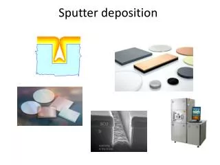
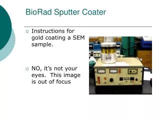
The Key System • The Key system has a stainless steel bell jar, a cryopump, gas supply system, four 2" targets and a substrate holder for six substrates. • The cycle time is about one day--it takes a day to load substrates and targets and reach the starting pressure for deposition. • We will use three cycles to produce a set of test samples. ref: www.lesker.com
We will use native oxide coated Si wafers--the surface is basically glass (amorphous SiOx). Currently Si(100) is less expensive than glass. Si(100) is easy to cleave along high symmetry planes to make smaller samples. The four targets are Ta, Cu, permalloy (Ni80Fe20), and silicon nitride (Si3N4). We will produce single layers, superlattices and multilayers for characterization using the methods available in the center. First the fluxes will be calibrated, then the test samples will be fabricated. Targets and Substrates
Si • Si forms in the diamond structure--two interpenetrating fcc lattices, one displaced by (1/4 1/4 1/4). • Si is semiconducting. • The surface is an amorphous oxide similar in structure and composition to glass. • A H-terminated single crystal surface can be produced by wet etching the oxide in HF. http://cst-www.nrl.navy.mil/lattice/mainpage.html
Ta • Tantalum is formed in the body centered cubic structure. • Tantalum is a refractory metal with a high melting point and low reactivity so it makes a good "capping layer." • The surface energy is high, so other metals with lower surface energy completely wet the surface. • Ta reacts strongly with Si to form a silicide interface layer which bonds the film strongly to the substrate. http://cst-www.nrl.navy.mil/lattice/mainpage.html
Cu • Cu forms in the fcc lattice structure. • Cu is the ubiquitous conductor, with applications wherever a low resistance current path is needed. • Cu has a relatively low surface energy for a metal and low reactivity with SiOx. • Cu oxidizes slowly in air, so it makes a marginal "capping layer." http://cst-www.nrl.navy.mil/lattice/mainpage.html
Ni80Fe20 • Permalloy is a random substitutional alloy which forms in the fcc phase with a lattice constant nearly equal to that of Cu. • Permalloy is a soft magnet, with coercivity and anisotropy dependent on deposition conditions. • The surface energy is comparable to Cu with a moderate reactivity with Si. • The Ni and Fe oxidize to form a nonmagnetic surface layer. http://cst-www.nrl.navy.mil/lattice/mainpage.html
Si3N4 • Silicon nitride forms in a hexagonal phase, however in thin film form it is usually amorphous. • It is a high temperature ceramic, with a larger bandgap than pure Si. • The surface energy is comparable to SiOx-- much lower than that of a typical metal. • It makes a good capping layer because it is inert. http://cst-www.nrl.navy.mil/lattice/mainpage.html
Load targets--2" diameter disks of the pure materials. Cleave substrates and mark for later lift-off of film for thickness measurement. Load substrates. Initiate pump down procedure. After crossover point is reached, you may leave the room until the starting pressure is reached (hours). Deposit thick films at stable pressure and power for a measured deposition time for flux calibration. Load new substrates and measure thicknesses with the profilimeter. Deposit films with specific thicknesses using the flux calibration data. Procedure
Effect of Ta underlayer on permalloy and Cu crystal texture. Smooth versus rough layers for AFM comparison. A multilayer with high optical contrast for ellipsometry study. Thin permalloy films with different capping layers. Superlattices for x-ray reflectivity (High Z/Low Z)xn for high x ray contrast. Single crystal Cu or permalloy on H-Si(100). Suggested Samples