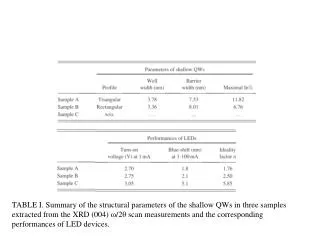
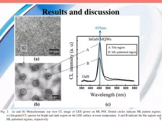
Download
1 / 1
10 likes | 155 Vues
This research investigates the sputter deposition of thin film composites, focusing on creating superior coatings that withstand severe conditions such as high temperatures and friction. Utilizing a range of methodologies, including atomic force microscopy (AFM), tribometry, and laser profilometry, the study evaluates the thickness and wear properties of multilayer coatings, particularly Titanium Nitride (TiN) and Tungsten Disulfide (WS2). Research findings emphasize the control over thin film thickness, revealing challenges and variances in measurement accuracy, while demonstrating potential applications in enhancing material performance.

E N D
Sputter Deposition of Thin Film CompositesJack Stransky1, Sriram Sundararajan21 Deparment of Chemistry University of Wisconsin - Stout2Department of Mechanical Engineering, Iowa Sate University Results and Discussion • According to previous research1 these settings would deposit a coating of 100nm • Sputter deposition typically produces even films • Atomic Force Microscope –Thin film thickness analysis • Profilometer – Thin film thickness analysis • Tribometer • Frictional and wear force testing of planar thin films • 100 nN minimum normal force • Contact profilometry step height results • Step heights of thin films showed high variance between trials using this method • Showed film thicknesses of hundreds of nanometers with hundred nanometer standard deviation between step heights taken of the same sample • Measurements not considered accurate because it may have measured a buildup of material cause by creation of the step making it not representative of the sample itself Introduction and Motivation Objectives Materials • Ever-growing need for superior coatings able to withstand severe operating conditions, including high temperatures, to have low friction, and to last longer. • Multicomponent coatings can combine desired properties from different components • Multilayer coating • Multiphase coating • Thin films can be produced using various methods such sputter deposition which allows for deposition of layers of different materials. • Depositmultilayer thin films using sputter coating • Titanium Nitride (TiN)3 • Tungsten Disulfide (WS2)1 • Investigate optimal sputter deposition parameters for samples • Perform friction and wear analysis on planar samples and atomic surface analysis of needle samples • Sputtering targets • Titanium Nitride (TiN) - strong, wear resistant, high melting point 3 • Tungsten Disulfide (WS2) - solid state lubricant (low coefficient of friction), high melting point 1 • Methods • Electropolisher – Needle sample preparation • Etches wire to microscale sharpness using an electrolyte • Voltage is applied to electrolyte and wire • Sputter Coater – Thin film deposition • WS2 and TiN targets deposited on glass substrate • Deposition rate unknown • Sputter coater power settings from 100-200 W, argon partial pressure was from 8-16 mTorr, and sputter coating was done for 15 minutes. Figure 3: AFM images of a few nm step in a thin film of WS2 • AFM step height results • Found thin film heights to be~5nm • Growth rate would then be ~1/3 nm/min • Non contact Laser profilometry step height results • Laser profilometer showed much lower step heights as well. • Samples heights found to be ~10nm • Atom probe needle sample preparation • Tips were prepared by etching tungsten wire in 5% NaOH electrolyte while 4V DC was applied for around 15 minutes. 20 tips were made using this method. • Tribometer tests at normal loads of 100,300,500, and 700nN destroyed the probe • Tips intended for atom probe use are unusable for friction and wear testing on the tribometer • Very thin layers of tungsten disulfide were produced • Growth rate was <1nm/min meaning that the thin film thickness of tungsten disulfide can be well controlled through sputter coating. • 1 Scharf, T.W.; Rajendran A.; Banerjee. B.; Sequeda, F. Growth structure and friction behavior of titanium doped tungsten disulphide (Ti-WS2) nanocomposite thin films. Thin Solid Films. 2009,517, 5666-5675. • 2 Miller, M.K Atom Probe Tomography: Analysis at the Atomic Level;Kluwer Academic/Plenum: New York, 2000 • 3 Stone, D. S.; K. B. Yoder; W. D. Sproul "Hardness and elastic modulus of TiN based on continuous indentation technique and new correlation". Journal of Vacuum Science and Technology, 1991,9 2543–2547. Figure 1: Electropolishing schematic 2 Figure 2: Sputter Coating system Figure 4:Atom probe tip at 500x magnification Conclusions References Table 1: Contact profilometer data. Ra and step size are in angstroms