Single-cycle Multi-cycle FSM controller Multi-cycle microcontroller
EECS 322: Computer Architecture. Single-cycle Multi-cycle FSM controller Multi-cycle microcontroller. MIPS instruction formats. 1. I. m. m. e. d. i. a. t. e. a. d. d. r. e. s. s. i. n. g. 2. R. e. g. i. s. t. e. r. a. d. d. r. e. s. s. i. n. g. R. e. g.

Single-cycle Multi-cycle FSM controller Multi-cycle microcontroller
E N D
Presentation Transcript
EECS 322: Computer Architecture Single-cycleMulti-cycle FSM controllerMulti-cycle microcontroller CWRU EECS 322 March 6, 2000
MIPS instruction formats 1 . I m m e d i a t e a d d r e s s i n g 2 . R e g i s t e r a d d r e s s i n g R e g i s t e r s R e g i s t e r 3 . B a s e a d d r e s s i n g M e m o r y B y t e H a l f w o r d W o r d R e g i s t e r 4 . P C - r e M e m o r y W o r d M e m o r y W o r d o p r s r t I m m e d i a t e Arithmetic add $rd,$rs,$rt o p r s r t r d . . . f u n c t Data Transfer lw $rd,offset($rs) sw $rd,offset($rs) o p r s r t A d d r e s s + l a t i v e a d d r e s s i n g o p r s r t A d d r e s s Conditional branch beq $rd,$rs,raddr + P C 5 . P s e u d o d i r e c t a d d r e s s i n g Unconditional jump j addr o p A d d r e s s P C CWRU EECS 322 March 6, 2000
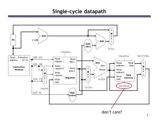
Single Cycle Implementation • Calculate instruction cycle time assuming negligible delays except: • memory (2ns), ALU and adders (2ns), register file access (1ns) Adder2: PCPC+signext(IR[15-0]) <<2 Adder3: Arithmetic ALU Adder1: PC PC + 4 Single Cycle = 2 adders + 1 ALU CWRU EECS 322 March 6, 2000
Single/Multi-Clock Comparison add = 6ns = Fetch(2ns)+RegR(1ns)+ALU(2ns)+RegW(2ns) lw = 8ns = Fetch(2ns)+RegR(1ns)+ALU(2ns)+MemR(2ns)+RegW(2ns) sw = 7ns = Fetch(2ns)+RegR(1ns)+ALU(2ns)+MemW(2ns) beq = 5ns = Fetch(2ns)+RegR(1ns)+ALU(2ns) j = 2ns = Fetch(2ns) Architectural improved performance without speeding up the clock! CWRU EECS 322 March 6, 2000
Some Design Trade-offs High level design techniques Algorithms: change instruction usage minimize ninstruction * tinstruction Architecture: Datapath, FSM, Microprogramming adders: ripple versus carry lookahead multiplier types, … Lower level design techniques (closer to physical design) clocking: single verus multi clock technology: layout tools: better place and route process technology: 0.5 micron to .18 micron CWRU EECS 322 March 6, 2000
Single-cycle problems • Single Cycle Problems: • what if we had a more complicated instruction like floating point? (fadd = 30ns, fmul=100ns) • wasteful of area (2 adders + 1 ALU) • One Solution: • use a “smaller” cycle time (if the technology can do it) • have different instructions take different numbers of cycles • a “multicycle” datapath (1 ALU) • Multi-cycle approach • We will be reusing functional units: ALU used to increment PC (Adder1) and to compute address (Adder2) • Memory used for instruction and data CWRU EECS 322 March 6, 2000
Reality Check: Intel 8086 clock cycles Arithmetic 3 add reg16, reg16 118-133 mul dx:ax, reg16 very slow!! 128-154 imul dx:ax, reg16 114-162 div dx:ax, reg16 165-184 idiv dx:ax, reg16Data Transfer 14 mov reg16, mem16 15 mov mem16, reg16Conditional Branch 4/16 je displacement8Unconditional Jump 15 jmp segment:offset16 CWRU EECS 322 March 6, 2000
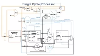
Multi-cycle Datapath Multi-cycle = 1 ALU + Controller CWRU EECS 322 March 6, 2000
Multi-cycle Datapath: with controller CWRU EECS 322 March 6, 2000
Multi-cycle: 5 execution steps • T1 (a,lw,sw,beq,j) Instruction Fetch • T2 (a,lw,sw,beq,j) Instruction Decode and Register Fetch • T3 (a,lw,sw,beq,j) Execution, Memory Address Calculation, or Branch Completion • T4 (a,lw,sw) Memory Access or R-type instruction completion • T5 (a,lw) Write-back step INSTRUCTIONS TAKE FROM 3 - 5 CYCLES! CWRU EECS 322 March 6, 2000
Multi-cycle Approach All operations in each clock cycle Ti are done in parallel not sequential! For example, T1, IR = Memory[PC] and PC=PC+4 are done simultaneously! T1 T2 T3 T4 T5 Between Clock T2 and T3 the microcode sequencer will do a dispatch 1 CWRU EECS 322 March 6, 2000
Multi-cycle using Microprogramming Microcode controller Finite State Machine( hardwired control ) M i c r o c o d e s t o r a g e C o m b i n a t i o n a l c o n t r o l l o g i c D a t a p a t h c o n t r o l o u t p u t s D a t a p a t h c o n t r o l O u t p u t s firmware o u t p u t s O u t p u t s I n p u t 1 I n p u t s S e q u e n c i n g M i c r o p r o g r a m c o u n t e r c o n t r o l A d d e r N e x t s t a t e A d d r e s s s e l e c t l o g i c I n p u t s f r o m i n s t r u c t i o n S t a t e r e g i s t e r r e g i s t e r o p c o d e f i e l d I n p u t s f r o m i n s t r u c t i o n r e g i s t e r o p c o d e f i e l d Requires microcode memory to be faster than main memory CWRU EECS 322 March 6, 2000
Microcode: Trade-offs • Distinction between specification and implementation is sometimes blurred • Specification Advantages: • Easy to design and write (maintenance) • Design architecture and microcode in parallel • Implementation (off-chip ROM) Advantages • Easy to change since values are in memory • Can emulate other architectures • Can make use of internal registers • Implementation Disadvantages, SLOWER now that: • Control is implemented on same chip as processor • ROM is no longer faster than RAM • No need to go back and make changes CWRU EECS 322 March 6, 2000
Microinstruction format CWRU EECS 322 March 6, 2000
Microinstruction format: Maximally vs. Minimally Encoded • No encoding: • 1 bit for each datapath operation • faster, requires more memory (logic) • used for Vax 780 — an astonishing 400K of memory! • Lots of encoding: • send the microinstructions through logic to get control signals • uses less memory, slower • Historical context of CISC: • Too much logic to put on a single chip with everything else • Use a ROM (or even RAM) to hold the microcode • It’s easy to add new instructions CWRU EECS 322 March 6, 2000
Microprogramming: program CWRU EECS 322 March 6, 2000
Microprogramming: program overview T1 T2 T3 T4 T5 Fetch Fetch+1 Dispatch 1 Rformat1 BEQ1 JUMP1 Mem1 Dispatch 2 Rformat1+1 LW2 SW2 LW2+1 CWRU EECS 322 March 6, 2000
Microprogram steping: T1 Fetch (Done in parallel) IRMEMORY[PC] & PC PC + 4 Label ALU SRC1 SRC2 RCntl Memory PCwrite SeqFetch add pc 4 ReadPCALU Seq CWRU EECS 322 March 6, 2000
T2 Fetch + 1 AReg[IR[25-21]] & BReg[IR[20-16]] & ALUOutPC+signext(IR[15-0]) <<2 Label ALU SRC1 SRC2 RCntl Memory PCwrite Seq add pc ExtSh Read D#1 CWRU EECS 322 March 6, 2000
T3 Dispatch 1: Mem1 ALUOut A + sign_extend(IR[15-0]) Label ALU SRC1 SRC2 RCntl Memory PCwrite SeqMem1 add A ExtSh D#2 CWRU EECS 322 March 6, 2000
T4 Dispatch 2: LW2 MDR Memory[ALUOut] Label ALU SRC1 SRC2 RCntl Memory PCwrite SeqLW2 ReadALU Seq CWRU EECS 322 March 6, 2000
T5 LW2+1 Reg[ IR[20-16] ] MDR Label ALU SRC1 SRC2 RCntl Memory PCwrite SeqWMDR Fetch CWRU EECS 322 March 6, 2000
T4 Dispatch 2: SW2 Memory[ ALUOut ] B Label ALU SRC1 SRC2 RCntl Memory PCwrite SeqSW2 WriteALU Fetch CWRU EECS 322 March 6, 2000
T3 Dispatch 1: Rformat1 ALUOut A op(IR[31-26]) B op(IR[31-26]) Label ALU SRC1 SRC2 RCntl Memory PCwrite SeqRf...1 op A B Seq CWRU EECS 322 March 6, 2000
T4 Dispatch 1: Rformat1+1 Reg[ IR[15-11] ] ALUOut Label ALU SRC1 SRC2 RCntl Memory PCwrite Seq WALU Fetch CWRU EECS 322 March 6, 2000
T3 Dispatch 1: BEQ1 If (A - B == 0) { PC ALUOut; } ALUOut = Address computed in T2 ! Label ALU SRC1 SRC2 RCntl Memory PCwrite SeqBEQ1 subt A B ALUOut-0 Fetch CWRU EECS 322 March 6, 2000
T3 Dispatch 1: Jump1 PC PC[31-28] || IR[25-0]<<2 Label ALU SRC1 SRC2 RCntl Memory PCwrite SeqJump1 Jaddr Fetch CWRU EECS 322 March 6, 2000
The Big Picture CWRU EECS 322 March 6, 2000