Download
1 / 26
270 likes | 425 Vues
Motivation. problem: global warming and climate change. Contents. Introduction Material Properties Growth Methods for Thin Films Development of CIGS Thin Film Solar Cells Fabrication Technology Conclusion & Prospect. Introduction. CIS = CuInSe 2 (copper indium diselenide)

E N D
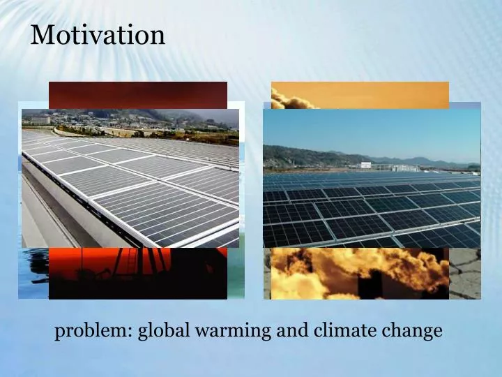
Motivation problem: global warming and climate change
Contents • Introduction • Material Properties • Growth Methods for Thin Films • Development of CIGS Thin Film Solar Cells • Fabrication Technology • Conclusion & Prospect
Introduction • CIS = CuInSe2 (copper indium diselenide) CIGS = CuInxGa1-xSe2 (copper indium gallium diselenide) • compound semiconductor ( I-III-VI) • heterojunction solar cells • high efficiency (≈19% in small area, ≈13% in large area modules) • very good stability in outdoor tests • applications: • solar power plants • power supply in aerospace • decentralized power supply • power supply for portable purposes
Contents • Introduction • Material Properties • Phase diagram • Impurities & Defects • Growth Methods for Thin Films • Development of CIGS Thin Film Solar Cells • Fabrication Technology • Conclusion & Prospect
Material Properties I • crystal structure: • tetragonal chalcopyrite structure • derived from cubic zinc blende structure • tetrahedrally coordinated • direct gap semiconductor • band gap: 1.04eV – 1.68eV • exceedingly high adsorptivity • adsorption length: >1µm • minority-carrier lifetime: several ns • electron diffusion length: few µm • electron mobility: 1000 cm2 V -1 s-1 (single crystal)
Material Properties II • simplified version of the ternary phase diagram • reduced to pseudo-binary phase diagram along the red dashed line • bold black line: photovoltaic-quality material • 4 relevant phases: a-, b-, d-phase and Cu2Se Hamakawa, Yoshihiro: Thin Film Solar Cells, Springer, 2004.
Material Properties III • a-phase(CuInSe2): • range @RT: 24-24.5 at% • optimal range for efficient thin film solar cells: 22-24 at % • possible at growth temp.: 500-550°C, @RT: phase separation into a+b • b-phase(CuIn3Se5) • built by ordered arrays of defect pairs ( áVCu, InCuñ anti sites) • d-phase(high-temperature phase) • built by disordering Cu&In sub-lattice • Cu2Se • built from chalcopyrite structure by Cu interstitials Cui & CuIn anti sites Hamakawa, Yoshihiro: Thin Film Solar Cells, Springer, 2004.
Impurities & Defects I problem: a-phase highly narrowed @RT • solution: widening a-phase region by impurities • partial replacement of In with Ga • 20-30% of In replaced • Ga/(Ga+In) »0.3 Þband gap adjustment • incorporation of Na • 0.1 at % Na by precursors Þbetter film morphology Þpassivation of grain-boundaries Þhigher p-type conductivity Þreduced defect concentration Hamakawa, Yoshihiro: Thin Film Solar Cells, Springer, 2004.
Impurities & Defects II • doping of CIGS with native defects: • p-type: • Cu-poor material, annealed under high Se vapor pressure • dominant acceptor: VCu • problem: VSe compensating donor • n-type: • Cu-rich material, Se deficiency • dominant donor: VSe • electrical tolerance to large-off stoichiometries • nonstoichiometry accommodated in secondary phase • off-stoichiometry related defects electronically inactive
Impurities & Defects III • electrically neutral nature of structural defects • Efdefect complexes < Efsingle defect Þ formation of defect complexes out of certain defects á2VCu, InCuñ, áCuIn, InCuñ and á2Cui, InCuñ • no energy levels within the band gap • grain-boundaries electronically nearly inactive
Contents • Introduction • Material Properties • Growth Methods for Thin Films • Coevaporation process • Sequential process • Roll to roll deposition • Development of CIGS Thin Film Solar Cells • Fabrication Technology • Conclusion & Prospect
Growth Methods for Thin Films I coevaporation process: • evaporation of Cu, In, Ga and Se from elemental sources • precise control of evaporation rate by EIES & AAS or mass spectrometer • required substrate temperature between 300-550°C • inverted three stage process: • evaporation of In, Ga, Se • deposition of (In,Ga)2Se3 on substrate @ 300°C • evaporation of Cu and Se deposition at elevated T • evaporation of In, Ga, Se Þsmoother film morphology Þ highest efficiency Hamakawa, Yoshihiro: Thin Film Solar Cells, Springer, 2004.
Growth Methods for Thin Films II sequential process: • selenization from vapor: • substrate: soda lime glass coated with Mo • deposition of Cu and In, Ga films by sputtering • selenization under H2Se atmosphere • thermal process for conversion into CIGS advantage: large-area deposition disadvantage: use of toxic gases (H2Se) • annealing of stacked elemental layers • substrate: soda lime glass coated with Mo • deposition of Cu and In, Ga layers by sputtering • deposition of Se layer by evaporation • rapid thermal process advantage: large-area deposition avoidance of toxic H2Se Hamakawa, Yoshihiro: Thin Film Solar Cells, Springer, 2004.
Mo Cu,Ga,In,Se CdS ZnO Growth Methods for Thin Films III roll to roll deposition: • substrate: polyimide/ stainless steel foil coated with Mo • ion beam supported low temperature deposition of Cu, In, Ga & Se advantages: low cost production method flexible modules and high power per weight ratio disadvantages: lower efficiency http://www.solarion.net/images/uebersicht_technologie.jpg
Contents • Introduction • Material Properties • Growth Methods for Thin Films • Development of CIGS Thin Film Solar Cells • Cross section of a CIGS thin film • Buffer layer • Window layer • Band-gap structure • Fabrication Technology • Conclusion & Prospect
Development of CIGS Solar Cells I Zn0 front contact 0.5µm CdS buffer 50nm CIGS absorber 1.6 µm Mo back contact 1µm soda lime glass substrate 2mm www.kolloquium-erneuerbare-energien.uni-stuttgart.de/downloads/Kolloq_2006/Dimmler_EEKolloq-290606.pdf
Development of CIGS Solar Cells II Buffer layer: CdS • deposited by chemical bath deposition (CBD) • layer thickness: 50 nm properties: • band gap: 2.5 eV • high specific resistance • n-type conductivity • diffusion of Cd 2+ into the CIGS-absorber (20nm) • formation of CdCu- donors, decrease of recombination at CdS/CIGS interface function: • misfit reduction between CIGS and ZnO layer • protection of CIGS layer Hamakawa, Yoshihiro: Thin Film Solar Cells, Springer, 2004.
Development of CIGS Solar Cells III Window layer: ZnO • band gap: 3.3 eV • bilayer high- / low-resistivity ZnO deposited by RF-sputtering / atomic layer deposition (ALD) • resistivity depending on deposition rate (RF-sputtering)/flow rate (ALD) • high-resistivity layer: • layer thickness 0.5µm • intrinsic conductivity • low-resistivity layer: • highly doped with Al(1020 cm-3) • n-type conductivity function: • transparent front contact R.Menner, M.Powalla: Transparente ZnO:Al2O3 Kontaktschichten für CIGS Dünnschichtsolarzellen
Development of CIGS Solar Cells IV band gap structure: • i-ZnO inside space-charge region • discontinuities in conduction band structure • i-ZnO/CdS: 0.4eV • CdS/CIGS: - 0.4eV –0.3eV depends on concentration of Ga • positive space-charge at CdS/CIGS • huge band discontinuities of valance-band edge • electrons overcome heterojunction exclusively • heterojunction: n+ip Meyer, Thorsten: Relaxationsphänomene im elektrischen Transport von Cu(In,Ga)Se2, 1999.
Contents • Introduction • Material Properties • Growth Methods for Thin Films • Development of CIGS Thin Film Solar Cells • Fabrication Technology • Cell processing • Module processing • Conclusion & Prospect
substrate Fabrication Technology I cell processing: • substrate wash #1 • deposition of metal base electrode • patterning #1 • formation of p-type CIGS absorber • monolithical integration: • during cell processing • fabrication of complete modules • deposition of buffer layer • patterning #2 • deposition of n-type window layer • patterning#3 • deposition Ni/Al collector grid • deposition of antireflection coating Hamakawa, Yoshihiro: Thin Film Solar Cells, Springer, 2004.
ethylene vinyl acetate (EVA) as pottant tempered glass as cover glass soda-lime glass as substrate Al frame junction box with leads CIGS-based circuit Fabrication Technology II module processing: • packaging technology nearly identical to crystalline-Si solar cells Hamakawa, Yoshihiro: Thin Film Solar Cells, Springer, 2004.
Contents • Introduction • Material Properties • Growth Methods for Thin Films • Development of CIGS Thin Film Solar Cells • Fabrication Technology • Conclusion & Prospect
Conclusion & Prospects conclusion: • high reliability • high efficiency (≈19% in small area, ≈13% in large area modules) • less consumption of materials and energy • monolithical integration • high level of automation prospects: • increasing utilization (solar parks, aerospace etc.) • optimization of fabrication processes • gain in efficiency for large area solar cells • possible short run of indium and gallium resources http://img.stern.de/_content/56/28/562815/solar1_500.jpg www.kolloquium-erneuerbare-energien.uni-stuttgart.de/downloads/Kolloq_2006/Dimmler_EEKolloq-290606.pdf
Thank you for your attention! References: Hamakawa, Yoshihiro: Thin Film Solar Cells, Springer, 2004. Meyer, Thorsten: Relaxationsphänomene im elektrischen Transport von Cu(In,Ga)Se2, 1999. Dimmler, Bernhard: CIS-Dünnschicht-Solarzellen Vortrag, 2006.