Download
1 / 20
200 likes | 325 Vues
Simultaneous Photon Counting and Charge Integrating Readout Electronics for X-ray Imaging Hans Krüger, University of Bonn, Germany. University of Bonn: Michael Karagounis, Manuel Koch, Edgar Kraft, Hans Krüger, Norbert Wermes University of Mannheim: Peter Fischer, Ivan Peric

E N D
Simultaneous Photon Counting and Charge Integrating Readout Electronics for X-ray Imaging Hans Krüger, University of Bonn, Germany University of Bonn: Michael Karagounis, Manuel Koch, Edgar Kraft, Hans Krüger, Norbert Wermes University of Mannheim: Peter Fischer, Ivan Peric Philips Research Laboratories Aachen: Christoph Herrmann, Augusto Nascetti, Michael Overdick, Walter Rütten
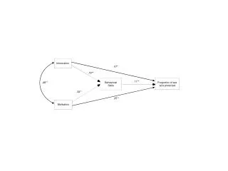
Motivation • Photon counting • limited to count rates < 10 MHz / pixel • Quantum limited noise statistics • Charge integration • High photon flux • does not reach quantum limited resolution at low photon flux Hans Krüger, University of Bonn
Counting and Integrating X-ray Detection (CIX) more information from the same x-ray dosage Integrator Photon counter signal intensity Hans Krüger, University of Bonn
Conversion Layer Total deposited energy Mean photon energy Integrating Channel Counting Channel Number of absorbed photons Preamp Pixel Concept Hans Krüger, University of Bonn
Implementation Hans Krüger, University of Bonn
Prototype chip CIX 0.1 chip features: • AMS 0.35 µm CMOS technology • area per electronics channel: 100 µm 547 µm • linear arrangement of 17 cells(no bump bond pads) 2 test pixels with access to sub-circuits, e.g. preamplifier analog output • in-pixel signal generation circuits(design for testability) • low noise digital logic (low-swing differential current steering logic, DCL) Hans Krüger, University of Bonn
Pixel Cell Block Diagram • Photon counting • preamp with continuous reset • replication of feedback current sourced to the integrator • Charge integration (I to F converter) • comparator output triggers charge pump (synchronous) • constant charge packet removed from integrator feedback capacitor Cint • number of pump cycles and timestamps for first and last cycle stored • Signal simulation • switched capacitor and switched current charge injection circuits • internal/external dc current source Hans Krüger, University of Bonn
UCINT Time320µs small current t UCINT Time(1/3)*320µs larger current t Frame=320µs Integrator: Charge Packet Counting fclk = 8 MHz pump cycles = 2 Time = 2560 Imeas[pkts./clk] = 1/2560 = 0,0004 fclk = 8 MHz pump cycles = 2 Time = 853 Imeas[pkts./clk] = 1/853 = 0,0012 Hans Krüger, University of Bonn
Feedback Circuit • 3 differential pairs: • continuous reset of the CSA feedback capacitor • signal replication to source the integrator • leakage current compensation leakage current compensation (slow) feedback (fast) Hans Krüger, University of Bonn
Charge injection circuits (chopper) • chopper 1+2: switched capacitors (~10 fF), connected to preamplifier input • current chopper: • switched current source (800 nA max.), connected to preamplifier or integrator input • minimal pulse duration ~30 ns • leakage current simulation • up to five load capacitors (~100 fF each) connected to preamplifier input Hans Krüger, University of Bonn
Integrator and Charge Pumps • switched capacitor charge pump: • dQ = (VDDA - VIntRef) · 240 fF, typical charge packet 1.8 · 106 e- (i.e. 140 60 keV photons or 170 photons at 120 keV tube spectrum) • 1.7µA maximal current throughput (at 6 MHz clock rate) • switched current charge pump • packet size controlled by IPump bias DAC and clock rate • VIntTh controls charge pump trigger level Hans Krüger, University of Bonn
Ibias in in out out Iload Load I U Load I U Ibias ½ Ibias Vlo Vhi Vload 'ideal' load characteristic Differential Current Mode Logic • Differential pair with constant bias current Ibias • loads generate low voltage swings by I to U conversion • An ‘ideal’ load characteristic: • Vhi level fixed at maximum possible input voltage (~VDD-Vth –VDsat) • Vlow level fixed by the voltage swing required to ‘fully’ switch the current in the cell (~200 mV) • plateau at ½ Ibias guarantees equal rise and fall times • and all this independent of the absolute value of Ibiasto match given loads and speed requirements CML principle (inverter) P. Fischer, E. Kraft, “Low swing differential logic for mixed signal applications”, Nucl. Instr. Meth. A 518 (2004) 511-514 Hans Krüger, University of Bonn
in bias VSS GND Implementation of the load circuit • Approximation of the ideal load circuit • NMOS operated as a current source with adjustable voltage VSS • diode connected NMOS (or pn-diode) to ground • Vhi increases only little with Ibias • Differential swing can be adjusted through VSS Load I U measured load characteristic Iload ½ Ibias Vlo Vhi Vload Hans Krüger, University of Bonn
Measurements Hans Krüger, University of Bonn
Photon Counter Performance Hans Krüger, University of Bonn
discretisation limit perfect 12-bit ADC Integrator Noise Performance Poisson SNR limit Hans Krüger, University of Bonn
Impact of the Feedback Circuit • noise performance not optimal but Poisson statistics limits SNR for real X-ray photon detection (60 keV X-rays, CdTe sensor, 320 µs frame time): • 100 pA 23 ph, sqrt(23) = 4,8 • 1 nA 226 ph, sqrt(226) = 15 • 10 nA 2260 ph, sqrt(2260) = 48 DIRECT injection via feedback Poisson SNR limit Hans Krüger, University of Bonn
200 nA integrator 12 nA 6 MHz max. pulse frequency overlap region 66 pA photon counter a single pulse 3 pA Total Dynamic Range Hans Krüger, University of Bonn
photon counter overload original pulse size integrator lower limit Reconstruction of the Mean Photon Energy total energy / photon count Hans Krüger, University of Bonn
Summary • A readout scheme which is capable of simultaneous counting and integrating absorbed X-ray quanta has been proposed and implemented • The multi-stage feedback circuit of the pre-amplifier mirrors the signal current to the integrator and provides leakage current compensation • A prototype chip has been submitted and tested and showed the feasibility of the concept • The simultaneous operation is fully functional though still impaired by the excess noise of the (not optimized) feedback network • A new test chip has been submitted and is currently under study • Acknowledgements: • Edgar Kraft for the animated ppt – sildes • References: • E. Kraft et al., “Counting and Integrating Readout for Direct Conversion X-ray Imaging - Concept, Realization and First Prototype Measurement”, Proceedings of the IEEE 2005 NSS/MIC • P. Fischer, E. Kraft, “Low swing differential logic for mixed signal applications”, Nucl. Instr. Meth. A 518 (2004) 511-514 Hans Krüger, University of Bonn