Chap 6. Sequential Circuits
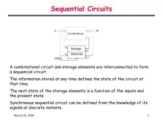
Chap 6. Sequential Circuits. Spring 2004 Jong Won Park jwpark@crow.cnu.ac.kr. 6-1 Sequential Circuit Definitions. sequential circuit combinational circuit + storage elements storage elements store binary information state of the sequential circuit at given state

Chap 6. Sequential Circuits
E N D
Presentation Transcript
Chap 6. Sequential Circuits Spring 2004 Jong Won Park jwpark@crow.cnu.ac.kr
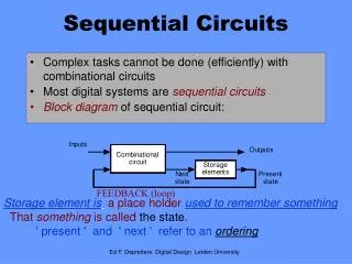
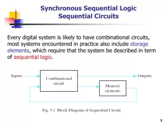
6-1 Sequential Circuit Definitions • sequential circuit • combinational circuit + storage elements • storage elements • store binary information state of the sequential circuit at given state • outputs are a function of the inputs & present state of the storage elements • next state of storage elements is also a function of the inputs & the present state Figure 6-1 Block Diagram of a Sequential Circuit
6-1 Sequential Circuit Definitions Figure 6-2 logic Structures for Strong Information
6-1 Sequential Circuit Definitions • two types • synchronous sequential circuit • behavior is defined from the knowledge of its signals at discrete instants of time • asynchronous sequential circuit • behavior depends on the inputs at any instance of time & the order in continuous time in which the inputs change, • clock generator • synchronous sequential circuit has a timing device • produce a periodic train of clock pulses • storage elements are affected only upon the arrival of each pulse • clock pulses are applied with other signals • the outputs can change their value only in the presence of clock pulses • clocked sequential circuits
6-1 Sequential Circuit Definitions • flip-flop • storage elements employed in clocked sequential circuits • a binary storage device capable of storing one bit of info • Normally, a sequential circuit uses many flip-flops • the transition from one state to the other occurs only at predetermined time intervals dictated by the clock pulses • two outputs: normal & complemented values Figure 6-3 Synchronous Clocked Sequential Circuit
6-2 Latches • A storage element can maintain a binary state indefinitely until directed by an input signal to switch states • Latch • most basic types of flip-flops • simple & most often used within flip-flops • used with more complex clocking methods to implement sequential circuits • SR Latch • a circuit with 2 cross-coupled NOR (or NAND) gates • 2 inputs: S (set) & R (reset)
6-2 Latches if S=1, Q=1 (Q'=0); if R=1, Q=0 (Q`=1) if S=R=0, keep previous state (hold) if S=R=1, undefined state Figure 6-4 SR Latch with NOR Gates Figure 6-5 Logic Simulatiom Of SR Latch Behavior
6-2 Latches • S'R' latch with two cross-coupled NAND gates • the input signals for the NAND require the complement of those values used for the NOR Figure 6-6 S’R’ Latch with NAND Gates
6-2 Latches • SR latch with a control input • a basic S'R' latch with 2 NAND gates • C (control input) acts as an enable signal for the other 2 inputs if C=0, no action; if C=1, act as SR f-f • the indeterminate condition (S=R=1) ==> seldom used in practice • but important, all others are constructed from it • SR latch with control input is called SR (or RS) f-f Figure 6-7 SR Latch with Control Input
6-2 Latches • D Latch • eliminate the undesirable condition of the indeterminate state • make S & R never equal to 1 at the same time ==> include an inverter • 2 inputs: D (data) & C (control) D goes to S; D' goes to R • act as a temporary storage • constructed with transmission gates Figure 6-8 D Latch Figure 6-9 D Latch with Transmission Gates
6-3 Flip-Flops • the state of a latch is allowed to switch by a momentary change of the control unit • a momentary change is called a trigger • a sequential circuit has a feedback path • control pulse goes to logic-1 • the new state of a latch may appear • the output is connected to the input • ...… Form a reliable flip-flop • master-slave flip-flop & edge-triggered flip-flop
6-3 Flip-Flops • Master-Slave Flip-Flop Figure 6-10 SR Master-Slave Flip-Flop Figure 6-11 Logic Simulation of an SR Master-Slave Flip-Flop
6-3 Flip-Flops Figure 6-12 Negative Edge-Triggered D Flip-Flop
6-3 Flip-Flops • Edge-Triggered Flip-flop • ignore the pulse while it is at a constant level, but triggers only during the transition of the clock signal Figure 6-13 Positive-Edge-Triggered D Flip-Flop
6-3 Flip-Flops Standard Graphics Symbols Figure 6-14 Standard Graphics Symbols for Latches and Flip-Flops
6-3 Flip-Flops • Direct Inputs • Preset and Clear inputs highly desirable !! Figure 6-15 D Flip-Flop with Direct Set and Reset
4.3 Flip-Flops • Flip-Flop Timing Figure 6-16 Flip-Flop Timing Parameters
6-4 Sequential Circuit Analysis • behavior of a sequential circuit is determined from inputs, outputs, & present state of the circuit • outputs & the next state are function of inputs & present state • Input Equations • a logic diagram of sequential circuit includes F-Fs (any type), or combinational circuit • the part of the combinational circuit can be described by a set of Boolean functions, called input equations
6-4 Sequential Circuit Analysis Sequential Circuit Analysis • Logic diagram • Input equations and output equations • State table • State diagram
6-4 Sequential Circuit Analysis DA = AX + BX, DB = A'X, Y = (A+B) X' (input equations for F-F) (equations for output Y) Figure 6-17 Example of a Sequential Circuit
6-4 Sequential Circuit Analysis • State Table • functional relationship between inputs, outputs, & flip-flop state • consist of 4 sections: present state, input, next state, output • list all possible combinations of present state and inputs • next state shows states of F-F one clock period later at time t+1 • State table example Table 6-1 State Table for Circuit of Figure 6-17
6-4 Sequential Circuit Analysis • State relationship A(t+1) = DA = AX + BX; B(t+1) = DB = A'X; Y = AX' + BX’ • Two-dimensional state table Table 6-2 Two-Dimensional State Table for the Circuit in Figure 6-17
6-4 Sequential Circuit Analysis • Mealy model • the outputs depend on the inputs and the states • Moore model • outputs depend only on the states (a 1-D column suffices) a Moore model circuit DA = A X Y, Z = A Figure 6-18 Logic Diagram and State Table for DA = A X Y
6-4 Sequential Circuit Analysis • State Diagram • The information (in a state table) may be represented graphically • state by a circle & transition between state by directed lines Figure 6-19 State Diagram • # sequential circuit of Fig 6-17 • binary number inside circle • = state of F-F • directed lines are labeled with (input/output) value • # sequential circuit of Fig 6-18 • one F-F with 2 states, 2 inputs, no output • directed lines are labeled w/ (input/output) value
6-4 Sequential Circuit Analysis • Sequential Circuit Timing Figure 6-20 Sequential Circuit Timing Parameters
6-4 Sequential Circuit Analysis • Sequential Circuit Timing tp= tslack + (tpd,FF + tpd,COMB + ts) tp≥ max (tpd,FF + tpd,COMB + ts) = tp ,min Figure 6-21 Sequential Circuit Timing Parths
6-4 Sequential Circuit Analysis • Ex6-1) Clock Period and Frequency Calculations 1.5ns= tslack + 0.2 +1.3 + 0.1 = tslack + 1.6ns • Simulation Figure 6-22 Simulation Timing
6-5 Sequential Circuit Design • combinational circuit: fully specified by a truth table • sequential circuit requires a state table for its specification • first step is to obtain a state table (or state diagram) • No. of F-F is determined from the no of states (up to 2n) • Design Procedure 1) Obtain the state diagram (from problem statement, or state diagram) 2) Obtain the state table 3) Assign binary codes to the states 4) Derive F-F input equations from next state conditions in table 5) Derive the output functions if needed 6) Simplify the input equations & output functions 7) Draw the logic diagram with D F-Fs & combinational gates
6-5 Sequential Circuit Design • Finding State Diagrams and State Tables Figure 6-23 Asynchronous and Synchronous Reset for D Flip-flops
6-5 Sequential Circuit Design • Finding State Diagram and State Tables Table6-3 State Table for State Diagram In Figure 6-21 Figure 6-24 Construction of a State Diagram for Example 6.2
6-5 Sequential Circuit Design • Ex6-3) Finding a State Diagram for a BCD-to-Excess-3 Decoder Table 6-4 Sequence Tables for Code Converter Example
6-5 Sequential Circuit Design Figure 6-25 Construction of a State Diagram for Example 6.3
6-5 Sequential Circuit Design Design Procedure 1) state diagram 2) state table 3) F-F input equationsandoutput functions 4) Simplify the input equations and output functions 5) logic diagram
6-5 Sequential Circuit Design • Sequence recognizer, 1101 Gray code를 할당함 A, B, C, D: 00,01,11,10 Figure 6-24 Construction of a State Diagram for Example 6.2
6-5 Sequential Circuit Design • Designing with D Flip-Flops(ABX로 truth table작성) Table 6-5 Table 6-3 with Names Replaced by Binary Codes
6-5 Sequential Circuit Design • A(t+1) = DA(A,B,X) = m(3,6,7) • B(t+1) = DB(A,B,X) = m(1,3,5,7) • Y(A,B,X) = m(5) Figure 6-26 Maps for Input Equations and Output Z
6-5 Sequential Circuit Design Figure 6-27 Logic Diagram for Sequential Circuit with D Flip-Flops
6-5 Sequential Circuit Design D Flip-Flops • Designing with Unused States • # A circuit with n F-F has 2n binary states • # unused states can be treated as don't care conditions Table 6-6 State Table for Designing with Unused States
6-5 Sequential Circuit Design D Flip-Flops Figure 6-28 Maps for Optimizing Input Equations
6-5 Sequential Circuit Design D Flip-Flops • Verification Figure 6-29 Test Sequence Generation for Simulation in Example 6.5
6-5 Sequential Circuit Design D Flip-Flops Figure 6-30 Simulation for Example 6.5
6-6 Other Flip-Flop Type • JK and T Flip-Flops Table 6-7 Flip-Flop Logic, Characteristic Tables and Equations, and Excitation Tables
6-7 HDL Representation for Sequential Circuits-VHDL • Ex6-5) VHDL for Positive-Edge-Triggered D Flip-Flop with Reset Figure 6-31 VHDL Process Description of Positive-Edge- Triggered Flip-Flop with Reset
6-7 HDL Representation for Sequential Circuits-VHDL • Ex6-6) VHDL for the Sequence Recognizer Figure 6-32 VHDL Process Description of a Sequence Recognizer
6-7 HDL Representation for Sequential Circuits-VHDL Figure 6-33 VHDL Process Description of a Sequence Recognizer (continued)
6-7 HDL Representation for Sequential Circuits-VHDL Table 6-8 Illustration of generation of storage in VHDL
6-8 HDL Representation for Sequential Circuits-Verilog • Ex6-7) Verilog for Positive-Edge-Triggered D Flip-Flop with Reset Figure 6-34 Verilog Process Description of Positive-Edge-Triggered Flip-Flop with Reset
6-8 HDL Representation for Sequential Circuits-Verilog • Ex6-8) Verilog for Sequence Recognizer Figure 6-35 Verilog Process Description of a Sequence Recognizer
6-8 HDL Representation for Sequential Circuits-Verilog Table 6-9 Illustration of generation of storage in Verilog

