Sequential Circuits
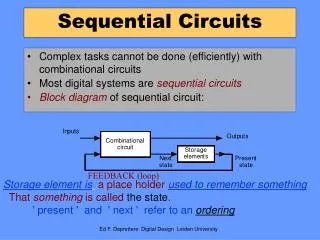
Complex tasks cannot be done (efficiently) with combinational circuits Most digital systems are sequential circuits Block diagram of sequential circuit:. Sequential Circuits. FEEDBACK (loop). Storage element is a place holder used to remember something

Sequential Circuits
E N D
Presentation Transcript
Complex tasks cannot be done (efficiently) with combinational circuits Most digital systems are sequential circuits Block diagram of sequential circuit: Sequential Circuits FEEDBACK (loop) Storage element isa place holderused to remember something That something is calledthe state. ' present ' and ' next ' refer to anordering Ed F. Deprettere Digital Design Leiden University
Place holder order 1 2 . . n n+1 . . Place holder releases current state and stores next state Current state at n+1 = next state at n place holders are built from FLIP-FLOPS which are built from latches Ed F. Deprettere Digital Design Leiden University
There is a gate delay (propagation delay, tpd) Example:buffer Do we need new gates? No, we don’tif we add Time to BehavioryieldingTimed Logic. A gate is built from physical transistors:it is causal ! i.e., output can not appear before or simultaneously with the input. (t) (t+tpd) X X Is logically possible, not physically: out istpdtime units laterthan in: in at time t , out at time t + tpd Ed F. Deprettere Digital Design Leiden University
Asynchronous and synchronous SCs Asynchronous:signals are defined at all timesTime is continuous Synchronous:signals at specific time instantsTime is discrete. Designing asynchronous sequential circuits is more difficult, yet not always avoidable ( sometimes even preferable) Flip-flopsare storage elements in synchronous circuits, but arethemselves constructed from asynchronous blocks calledLatches. The simplest latch is built from the buffer: 1/2tpd 1/2 tpd tpd Ed F. Deprettere Digital Design Leiden University
X(t) X(t+tpd) 1/2tpd tpd time (t) tpd tpd tpd Open & renew input Close & remove input Close t tpd What if I close the switch? Be carefull : tpd depends on technology! Ed F. Deprettere Digital Design Leiden University
States of flip-flops(memory elements) are set by clockpulses (no pulse, no state change even if input changes) All flip-flops are set at the same time (synchronous operation) Clocked Sequential Circuits Synchronous circuits that use a clock to synchronize. Time instances are at fixed distances. (! Synchronous is more general than clocked!) Ed F. Deprettere Digital Design Leiden University
Q is a name ! R S Q Q 2 3 4 1 SR Latch — Normal Operation The latched buffer is not very useful: information can not be changed. Replace the buffer’s inverter components by NORs or NANDs 1 active RESET 2 hold RESET 3 active SET 4 hold SET Ed F. Deprettere Digital Design Leiden University
Many flip-flops (latches) have two outputs Typical names are Q and Qbar Under most (normal) conditions, Qbar = Q', Q = Qbar'. When Q = 1 (Qbar = 0) the flip-flop is in the set state (the flip-flop is set) When Q = 0 (Qbar = 1) the flip-flop is in the resetstate The behavior of a flip-flop (latch) can be described with a function table (similar to truth table) Function table for SR latch Comments Ed F. Deprettere Digital Design Leiden University
S (set) Q Q R (reset) R Q R S Q Q Q S Q' R' Q' S' Rename: S' R R' S Q' Q Q' Q SR Latch SR latch is NOR basedSR latch is NAND based Play the circle-game S R S' R' Q Q Q' Q' 1 0 0 1 1 0 0 1 0 0 1 1 1 0 0 1 0 1 1 0 0 1 1 0 0 0 1 1 0 1 1 0 1 1 0 0 0 0 1 1 Ed F. Deprettere Digital Design Leiden University
SR latch with control input Getting better control on the latch SR latch Diagram Function Table Ed F. Deprettere Digital Design Leiden University
C Q D TG Q TG A good latch has well defined states and simple driving conditions The D Latch is such one. It’s behavior is very simple: Ed F. Deprettere Digital Design Leiden University
Block diagram The D Latch Is a real good latch: 1 control input, 1 data input well defined states Function Table D latch Ed F. Deprettere Digital Design Leiden University
A[k] sequent nextcurrentstate Flip-Flops The D latch can be used as aplace holder buth not in afeedback loop Why? Simple place holder take C=1 to get Q=A[k] then C=0 to hold. Feedback loop You want to read out the current and write in the next state at the same time instant:output (current state) must not see input (next state) as is the case with the D latch. Flip-flops are what we need. Ed F. Deprettere Digital Design Leiden University
Q P S S1 S2 C C1 C2 Q P R R1 R2 SR Master-Slave Flip-Flop Great?! Remember:SR latch may get into undefined state(oscillation danger) Master Latch Slave Latch Look at symbols Analysis: C = 0 —> C1 = 0, Current state Q not affected (remembered by M) —> C2 = 1, S copies current state Q to output P C = 1 —> C1 = 1, M reads next state (from S,R) —> C2 = 0, output of S not affected ( current state , P, remembered) Ed F. Deprettere Digital Design Leiden University
Analysis: S1 = JQbar, R1 = KQ J = 0, K = 0 —> S1, R1 = 0, State of M unchanged J = 1, K = 0: If Q = 1, State of M is unchanged (but since Q = 1, M is set). If Q = 0, S1 = 1, R1 = 0, M is set. Conclusion: M is set J = 0, K = 1: If Q = 0, State of M is unchanged from cleared state. If Q = 1, S1 = 0, S1 = 1, M is cleared. Conclusion: M is cleared J = 1, K = 1 —> S1 = Qbar, S2 = Q. State of M is reversed! Master-Slave JK Flip-Flop No undefined states. There are alternatives … Characteristic Table Ed F. Deprettere Digital Design Leiden University
Edge-triggered D Flip-Flops M latch S latch M latch S latch Data is copied into M when Clock = 1 The value of Data stored in M is whatever was present just before Clock goes from 1 to 0 Negative edge triggered FF Data is copied into M when Clock = 0 The value of Data stored in M is whatever was present just before Clock goes from 0 to 1 Positive edge triggered FF Ed F. Deprettere Digital Design Leiden University
Latches Positive control Negative control MS FF's Positive clock Negative clock Edge FF's 0-1 clock 1-0 clock Symbols and relations C(ontrol) is positive (negative) if it is active at logic 1 (0). Clock is positive or 'high' (negative or 'low') if no circle (if circle) appears at the C input. Ed F. Deprettere Digital Design Leiden University
Characteristic Tables Characteristic Table SR positive edge triggered flip-flop Triggered means clock control Table is same for negative edge triggered FF. In that case add circle external to C. Ed F. Deprettere Digital Design Leiden University
JK, D and T Flip-flops Characteristic Table JK negative edge triggered flip-flop Characteristic Table K = J' Negative clock master- slave D flip-flop Characteristic Table K = J Positive edge triggered T flip-flop Ed F. Deprettere Digital Design Leiden University
S R C J K Q Q 0 1 X X X 1 0 1 0 X X X 0 1 0 0 X X X 1 1 0 0 keep 1 1 0 1 0 1 1 1 1 0 1 0 1 1 1 1 flip S Q 1J C1 R 1K Flip-flops with asynchronous R In combinational circuits, we used enable bits to distinguish between operate and don’t operate. In sequential circuits, we use asynchronous S(et) and/or R(eset) Inputs to initialize states. IEEE standard notation Cn controls all nX inputs Circle: S is active at logic 0, so externally, you set with logic 1 (what you want) Ed F. Deprettere Digital Design Leiden University
Inputs Outputs Combinational circuit Flip-flops Clock pulses How to analyse sequential circuits Obviously more complicated than combinatorial circuits Two parts : combinational : no problem flip-flop part FF inputs depend on CC outputsbeing feedforward functions of CC inputs. FF outputs depend onFF inputs and Clock Hence on CC inputs and Clock. Ed F. Deprettere Digital Design Leiden University
A X D C B D clock C Y Be Systematic Inputs : X Outputs : Y States Variables : A, B Input Equations DA = AX+BX DB = A'X Output Equations Y = (A+B)X' Ed F. Deprettere Digital Design Leiden University
Inputs : X Outputs : Y States Variables : A, B Input Equations DA = AX+BX DB = A'X Output Equations Y = (A+B)X' State Table State Table Ed F. Deprettere Digital Design Leiden University
Characteristic Table T-ff Example: the counter Input equations T0 = 1, T1 = Q0, T2 = Q0Q1 Ed F. Deprettere Digital Design Leiden University
Is another way of writing state table Inputs : X Outputs : Y States Variables : A, B Input Equations DA = AX+BX DB = A'X Output Equations Y = (A+B)X' Two-Dimensional State Table 2D State Table Time trace Ed F. Deprettere Digital Design Leiden University
Write input equations for J, K inputs Find next state from JK characteristic table O.K ! K J K Q(t) Q(t+1) 0 0 0 0 1 0 0 1 1 J 1 1 1 0 1 0 0 0 1 1 0 Q 1 0 0 1 1 0 1 1 1 1 0 1 1 1 1 0 Analysis With JK Flip-Flops No change Reset Set Complement Q(t+1) = JQ'(t) + K'Q(t) O.K? Ed F. Deprettere Digital Design Leiden University
Inputs : X States Variables : A, B Input equations JA = B, KA = BX' JB = X', KB = AX'+A'X Present State Input Flip-flop inputs Next state A B X JA KA JB KB A B 0 0 0 0 0 1 0 0 1 0 0 1 0 0 0 1 0 0 0 1 0 1 1 1 0 1 1 0 1 1 1 0 0 1 1 0 1 0 0 0 0 1 1 1 1 1 0 1 0 0 0 0 1 0 1 1 0 1 1 1 1 0 0 1 1 1 1 0 0 0 1 1 Example with JK Flip-flops First + Third = State Table JQ' + K' Q What is known Input Equations Ed F. Deprettere Digital Design Leiden University
Finite State Machines (FSM) FSM is one of many so-calledmodels of computation. It is a graph G = (N, A), where Nis a set of nodesand Ais a set of arcs. Nodesrepresentstates Arcsrepresent transition between states The number of states, as well as the number of possible transitions between the states are finite. Hence the name. Ed F. Deprettere Digital Design Leiden University
1/0 0/0 Input 0/1 Output 0/1 0/1 1/0 1/0 1/0 State Diagrams The sequential circuits we have seen so far are FSMs. In digital design the FSM graphs are called state diagrams. They can be obtained straightforwardly from the state table Mealy Machine Outputs do depend on both inputs and present states. Very, very useful! Ed F. Deprettere Digital Design Leiden University
Inputs :X, Y State Variable : A Outputs : Z Input equation: DA = Exor(A, X, Y) Output Z = A inputs state/output 01,10 00,11 00,11 01,10 Moore Machine In aMoore Machinethe outputs only depends on the present states. Ed F. Deprettere Digital Design Leiden University
FSM example It is typically incontrol dominatedapplications that FSMs play a crucial role (traffic lights, automotive –dash board) A control dominatedapplication is typically given in plain English (requirements and constraints) – and the FSM is, then, a specificationfrom which an implementationis to be derived. Example: sequence recognizer Recognize the occurrence of the sequence 1101 in a long sequence of bits The long sequence is considered the input X. States are typically used to remember something about the past input. For example, the circuit must be in a state that remembers that the Three previous bits were 110. If, then, the input bit is one, the Occurrence of the sequence 1101 must be signaled (output Z) Ed F. Deprettere Digital Design Leiden University
1/0 1/0 0/0 A B C D FSM example (cont’d) X = ...010100110110100010101...1101.... 1/0 1/0 0/0 1/1 A B C D 0/0 1/0 0/0 1/1 0/0 Ed F. Deprettere Digital Design Leiden University