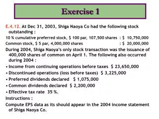
Exercise 1
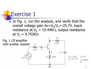
Exercise 1. In Fig. 1, run the analysis, and verify that the overall voltage gain Av=V 0 /V s =-25.74, input resistance at V S = 15.44K , output resistance at V o = 9.752K . Fig. 1 CE amplifier with emitter resistor. PSpice BJT Model. PSpice CE amplifier with emitter resistor.

Exercise 1
E N D
Presentation Transcript
Exercise 1 • In Fig. 1, run the analysis, and verify that the overall voltage gain Av=V0/Vs=-25.74, input resistance at VS = 15.44K, output resistance at Vo = 9.752K Fig. 1 CE amplifier with emitter resistor
PSpice BJT Model PSpice CE amplifier with emitter resistor
Question • What is the curve of Vo vs Vs when Vs value increases from 0mV to 1mV with 0.01mV.
Exercise 2 • In Fig. 2, run the analysis, and verify that the overall voltage gain Av=V0/Vi=-1.939, output resistance at Vo = 1.95K Fig.2 CS FET with Rs
Circuit Description by PSpice Common-Source FET with RS VI 1 0 1mV G 2 3 1 3 2mS RD 2 3 40K RL 2 0 2K RS 3 0 500 RG 1 2 10MEG .OP .OPT nopage .TF V(2) VI .END
Question • What is the curve of IL vs Vi when Vi value increases from 0mV to 1mV with 0.01mV?
Thinking….. • What is the simulation results when the Fig. 1 and Fig. 2 circuits are using real part for BJT and FET?