5.3 Sequential Circuits - An Introduction to Informatics -
150 likes | 321 Vues
5.3 Sequential Circuits - An Introduction to Informatics -. 2008. 11. 3 WMN Lab. Hey-Jin Lee. outline. Computer Organization Euclid’s Algorithm Sequential Circuits Shift Registers Sequential Adder Counters Sequential Circuit Design. Computer Organization. Storage Cell. Addressing

5.3 Sequential Circuits - An Introduction to Informatics -
E N D
Presentation Transcript
5.3 Sequential Circuits- An Introduction to Informatics - 2008. 11. 3 WMN Lab. Hey-Jin Lee
outline • Computer Organization • Euclid’s Algorithm • Sequential Circuits • Shift Registers • Sequential Adder • Counters • Sequential Circuit Design
Computer Organization Storage Cell Addressing 0000~9999 [ Instruction set ] operand operation code Console Input / Output Arithmetic Unit AC Control Unit IC Figure 1-16. Computer Organization
Euclid’s Algorithm Address Instruction Remarks 1.Compute remainder. 0201 + 1 1 0 0 0 AC ← m. 0202 + 4 1 0 0 1 AC ← AC – n (r - n) 0203 + 8 0 2 0 5 Transfer if ( r – n ) < 0 0204 + 5 0 2 0 2 Transfer back to 0202. 0205 + 3 1 0 0 1 Add n back in. 2. Test for termination 0206 + 6 0 2 1 3 Go to end if r = 0 0207 + 2 1 0 0 2 Store result in r. 3. Replace m by n and n by r. 0208 + 1 1 0 0 1 AC ← n 0209 + 2 1 0 0 0 m ← AC 0210 + 1 1 0 0 2 AC ← r 0211 + 2 1 0 0 1 n ← AC 0212 + 5 0 2 0 1 4. Return to main loop. 0213 + 0 0 0 0 0 5. Halt. Answer is in n. … … … 1000 + 0 0 0 2 0 Value of m 1001 + 0 0 0 0 8 Value of n 1002 + 0 0 0 0 0 Initial value of r Figure 1-23 : The Complete gcd Program
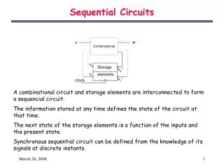
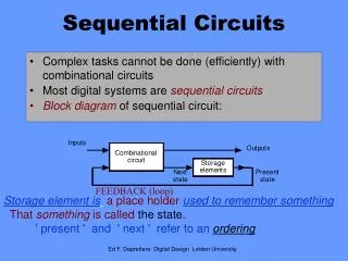
Sequential Circuits • What is the Sequential Circuits? • Circuit interconnected with combinational circuit and storage elements. • State Machine • Storage Elements • Circuit capable of storing binary information representing the state of the sequential circuits. n input m output Combinational Circuit Storage Element Present states Next states Flip- Flop Clock pulses
Shift registers • One important class of sequential circuits. • For example • Algoric If Shift then begin for i:= 0 upto 2 do X[ i] := X[ i+1 ]; x[3] := 0 end FF0 FF1 FF2 FF3 0 0 0 0 Shift 1 0 0 0 Shift 0 1 0 0 Shift 0 0 1 0 Shift 1 0 0 1 Figure 5-9 : Shift Register
Sequential Adder • Augend X, addend Y, and sum Z, the sum Z = X + Y can be obtained • with a single one-bit full adder (FA) and a flip-flop to store a carry bit. Figure 5-10 : Sequential Adder Block Diagram Figure 5-11 : Sequential Adder Algorithm Figure 5-11 : Sequential Adder Algorithm
Counters • This procedure can be generalized to implement ANY finite state machine • Counters are a very simple way to start: • no decisions on what state to advance to next current state is the output
Sequential Circuit Design • Step 1: Making a state table. • Step 2: Assigning binary codes to states. at least [ log2 n ] digits at least [ log2 n ] flip-flops. • Step 3: Finding flip-flop input values. • Step 4: Find simplified equations for the flip-flop inputs and the outputs. • Step 5: Build the circuit! • For example Recognizing a String of three One’s
next state input/output present state Sequential Circuit Design • Step 1: Making a state table. • Input string : 011001110000111111011110001111 • Output : 000000010000001001000100000010 • Step 1: Making a state table. • Input string : 011001110000111111011110001111 • Output : 000000010000001001000100000010 Figure 5-16 State Transition Graph
Sequential Circuit Design • Step 2: Assigning binary codes to states. State Transition Table
Sequential Circuit Design • Step 3: Finding flip-flop input values. • Use D flip-flop • You can just use the Next State columns
Sequential Circuit Design • Step 4: Find simplified equations for the flip-flop inputs and the outputs. DA = A’ • B • I DA = B • I DB = A’ • B’ • I O = A • B’ • I O=A • B’ • I + A • B • I =A • I
Sequential Circuit Design • Step 5: Build the circuit! DA = A’ • B • I DA = B • I DB = A’ • B’ • I O = A • B’ • I O = A • B’ • I + A • B • I = A • I Figure 5-18 Recognizing Strings of Three One’s
Q & A • Thank you.
