Download
1 / 21
280 likes | 666 Vues
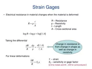
Strain Gages. Electrical resistance in material changes when the material is deformed. R – Resistance ρ – Resistivity l – Length A – Cross-sectional area. Taking the differential. Change in resistance is from change in shape as well as change in resistivity. For linear deformations.

E N D
Strain Gages • Electrical resistance in material changes when the material is deformed R – Resistance ρ – Resistivity l – Length A – Cross-sectional area Taking the differential Change in resistance is from change in shape as well as change in resistivity For linear deformations – strain Ss – sensitivity or gage factor (2-6 for metals and 40 – 200 for semiconductor)
Housing Output vo Strain Gage m Direction of Sensitivity (Acceleration) Seismic Mass Strain Member Cantilever Mounting Threads Base • The change in resistance is measured using an electrical circuit • Many variables can be measured – displacement, acceleration, pressure, temperature, liquid level, stress, force and torque • Some variables (stress, force, torque) can be determined by measuring the strain directly • Other variables can be measured by converting the measurand into stress using a front-end device Strain gage accelerometer
Strain gages are manufactured as metallic foil (copper-nickel alloy – constantan) Direction of Sensitivity Foil Grid Single Element Two-Element Rosette Backing Film Solder Tabs (For Leads) Three-Element Rosettes Semiconductor (silicon with impurity) Doped Silicon Crystal (P or N Type) Welded Gold Leads Nickle-Plated Copper Ribbons Phenolic Glass Backing Plate
Potentiometer or Ballast Circuit + v o Strain Gage Output R v ref - (Supply) Rc • Ambient temperature changes will introduce error • Variations in supply voltage will affect the output • Electrical loading effect will be significant • Change in voltage due to strain is a very small percentage of the output Question: Show that errors due to ambient temperature changes will cancel if the temperature coefficients of R and Rc are the same
Wheatstone Bridge Circuit A Small i + R1 vo R2 RL Load (High) R4 - R3 B - + vref (Constant Voltage) When the bridge is balanced True for any RL
Null Balance Method • When the stain gage in the bridge deforms, the balance is upset. • Balance is restored by changing a variable resistor • The amount of change corresponds to the change in stain • Time consuming – servo balancing can be used Direct Measurement of Output Voltage • Measure the output voltage resulting from the imbalance • Determine the calibration constant • Bridge sensitivity To compensate for temperature changes, temperature coefficients of adjacent pairs should be the same
The Bridge Constant • More than one resistor in the bridge can be active • If all four resistors are active, best sensitivity can be obtained • R1 and R4 in tension and R2 and R3 in compression gives the largest sensitivity • The bridge sensitivity can be expressed as Bridge Constant
Example 4.4 A strain gage load cell (force sensor) consists of four identical strain gages, forming a Wheatstone bridge, that are mounted on a rod that has square cross-section. One opposite pair of strain gages is mounted axially and the other pair is mounted in the transverse direction, as shown below. To maximize the bridge sensitivity, the strain gages are connected to the bridge as shown. Determine the bridge constant k in terms of Poisson’s ratiov of the rod material. Axial Gage 2 1 1 + vo Transverse Gage 2 3 − Cross Section Of Sensing Member 3 4 4 + − vref Transverse strain = (-v) x longitudinal strain
Calibration Constant k – Bridge Constant Ss – Sensitivity or gage factor
Example 4.5 A schematic diagram of a strain gage accelerometer is shown below. A point mass of weight W is used as the acceleration sensing element, and a light cantilever with rectangular cross-section, mounted inside the accelerometer casing, converts the inertia force of the mass into a strain. The maximum bending strain at the root of the cantilever is measured using four identical active semiconductor strain gages. Two of the strain gages (A and B) are mounted axially on the top surface of the cantilever, and the remaining two (C and D) are mounted on the bottom surface. In order to maximize the sensitivity of the accelerometer, indicate the manner in which the four strain gages A, B, C, and D should be connected to a Wheatstone bridge circuit. What is the bridge constant of the resulting circuit? A C Strain Gages A, B + δvo W − C, D D B l A b B + − C vref h D
Obtain an expression relating applied acceleration a (in units of g) to bridge output (bridge balanced at zero acceleration) in terms of the following parameters: • W = Mg = weight of the seismic mass at the free end of the cantilever element • E = Young’s modulus of the cantilever • l = length of the cantilever • b = cross-section width of the cantilever • h = cross-section height of the cantilever • Ss = gage factor (sensitivity) of each strain gage • vref = supply voltage to the bridge. • If M = 5 gm, E = 5x10¹⁰ N/m2, l = 1 cm, b = 1 mm, h = 0.5 mm, Ss = 200, and vref = 20 V, determine the sensitivity of the accelerometer in mV/g. • If the yield strength of the cantilever element is 5xl07 N/m2, what is the maximum acceleration that could be measured using the accelerometer? • If the ADC which reads the strain signal into a process computer has the range 0 to 10 V, how much amplification (bridge amplifier gain) would be needed at the bridge output so that this maximum acceleration corresponds to the upper limit of the ADC (10 V)? • Is the cross-sensitivity (i.e., the sensitivity in the two directions orthogonal to the direction of sensitivity small with this arrangement? Explain. • Hint: For a cantilever subjected to force F at the free end, the maximum stress at the root is given by
MEMS Accelerometer Signal Conditioning Mechanical Structure Applications: Airbag Deployment
AC Bridge Amplifier Demodulator And Filter Calibration Constant Dynamic Strain Strain Reading Oscillator Power Supply Data Acquisition • Supply frequency ~ 1kHz • Output Voltage ~ few micro volts – 1 mV • Advantages – Stability (less drift), low power consumption • Foil gages - 50Ω – kΩ • Power consumption decreases with resistance • Resolutions on the order of 1 m/m
Semiconductor Strain Gages Conductor Ribbons Single Crystal of Semiconductor Gold Leads Phenolic Glass Backing Plate • Gage factor – 40 – 200 • Resitivity is higher – reduced power consumption • Resistance – 5kΩ • Smaller and lighter
Disadvantages of Semiconductor Strain Gages • The strain-resistance relationship is nonlinear • They are brittle and difficult to mount on curved surfaces. • The maximum strain that can be measured is an order of magnitude smaller 0.003 m/m (typically, less than 0.01 m/m) • They are more costly • They have a much larger temperature sensitivity. Resistance Change Resistance Change P-type N-type 0.4 0.4 0.3 0.3 = 1 Microstrain = Strain of 1×10⁻⁶ 0.2 0.2 0.1 0.1 −3 −2 −1 1 2 3 −3 −2 −1 1 2 3 ×103 ×103 Strain −0.1 −0.1 Strain −0.2 −0.2 −0.3 −0.3
For semiconductor strain gages • S1 – linear sensitivity • Positive for p-type gages • Negative for n-type gages • Magnitude is larger for p-type • S2 – nonlinearity • Positive for both types • Magnitude is smaller for p-type
Linear Approximation Quadratic Curve Change in Resistance Linear Approximation Error −max max 0 Strain Quadratic Error Minimize Error = 0 Maximum Error
Range – change in resistance Percentage nonlinearity error
Temperature Compensation α = Temperature Coefficient of Resistance β = Temperature Coefficient of Gage Factor 3 α Compensation Feasible Temperature coefficients (per °F) 2 (−β) Compensation Not Feasible Compensation Feasible 1 0 Concentration of Trace Material (Atoms/cc) Resistance change due to temperature Sensitivity change due to temperature
Self Compensation with a Resistor R1 R R R2 + R R δvo − + − vi Rc R4 − + R3 Compensating Resistor Rc + − vref vi For self compensation the output after the temperature change must be the same vref Possible only for certain ranges