Download
1 / 5
60 likes | 221 Vues
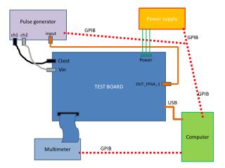
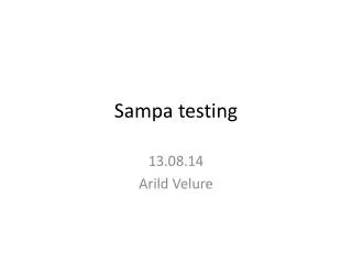
Test board development setup for the SAMPA Chip. FPGA Board to communicate with SAMPA test card. SAMPA test setup. FPGA Board to communicate with SAMPA test card. Test System ( Based on SoC kit - Cycnlon V). Key functions Provides reset & clocks of SAMPA chip Sampling clock (10-20 MHz)

E N D
Test board development setup for the SAMPA Chip FPGA Board to communicate with SAMPA test card
SAMPA test setup FPGA Board to communicate with SAMPA test card
Test System(BasedonSoCkit - Cycnlon V) • Key functions • Provides reset & clocks of SAMPA chip • Sampling clock (10-20 MHz) • B-X-ing clock (40 MHz) • Serial Link (320 MHz) • Hard Reset • Configuration • Read, write, and command transactions • Test Data (PRBS, fixed patterns e.t.c) • Test data Readout • Tapped (from BC1/BC2/TCFU …. E.t.c) • Full chained readout on SAMPA serial link HSMC Configuration Data Readout SoC-Kit Board
FPGA design • Communication / Interface • USB/UART: Serial Communication • Configurastion/ monitoring • Ethernet • Data transport link (DATE/DAQ) • HSMC • Link to SAMPA carrier board • In Lab test using HSMC adapter CONFG & COMM Control Module Memory NIOS II Clock Manager • Software/ DAQ • Labview / C # :- Serial Communication • Root / DATE :- DAQ, data analysis SoC-Kit Board
Plan & Current status • Hardware • One development board and HSMC to GPIO card is set-up in laboratory for development • Purchase order of two sets are sent to Terasic • Software / Firmware Development • Ganesh Tambave new post doc start working on User interface • Arild and Attiq work for specifications and firmware development