Memory
Memory. Semiconductor Memory. Memory refers to Semiconductor Memory. Hold digital information 0s and 1s. Memory. Workspace for processor. Temporary storage area where the programs and data being operated on by the processor reside.


Memory
E N D
Presentation Transcript
Semiconductor Memory • Memory refers to Semiconductor Memory. • Hold digital information 0s and 1s.
Memory • Workspace for processor. • Temporary storage area where the programs and data being operated on by the processor reside. • Starting a program brings the program files and data into RAM. The files and data remain in RAM as long as the program is running. • Main memory in a system is a collection of chips or modules that are plugged into the motherboard. • Chips must be compatible with the motherboard.
Semiconductor Memory • In the design of all computers, semiconductor memories are used as primary storage for code and data. • They are connected directly to the CPU and they are the memory that the CPU first asks for information (code and data). • For this reason, semiconductor memories are sometimes referred to as primary memory. • The main requirement of primary memory is that it must be fast in responding to the CPU
Types of Memory Two main types of memory used in PCs: • ROM (Read-Only Memory) • RAM (Random Access Memory)
Types of Memory • ROM: • PROM, • EPROM, • EEPROM, • Flash EPROM, and • Mask ROM • RAM: • SRAM (used as cache), • DRAM, and • NV-RAM
ROM • ROM is found on the motherboard plus on any devices that need to be accessed during startup. • Video cards • SCSI cards • Enhanced IDE controller cards • Network Interface cards
ROM • Motherboard ROM contains four main programs: • POST (power on self test). A series of test routines that test the system components. • CMOS Setup. A menu-driven application that allows the user to set system configuration parameters, options, security settings, and preferences. • Bootstrap Loader. The routine that scans the floppy disk and hard drive looking for an operating system to load. • BIOS (basic input/output system). Device drive programs that provided a standard interface to the other system hardware.
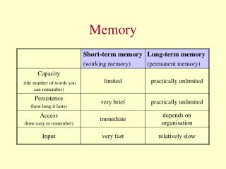
Characteristics of Memory • Capacity, • Organization, and • Speed
Memory Capacity of Computers/Chips • The number of bits that a computer/chip can store is called its capacity. • While the memory capacity of a memory IC chip is always given in bits, • The memory capacity of a computer is given in bytes. • 4M IC memory chip means 4 megabits. • 4M computer memory means 4 megabytes.
Speed • One of the most important characteristics of a memory chip is the speed at which data can be accessed from it. • To access the data, the address is presented to the address pins, and after a certain amount of time has elapsed, the data shows up at the data pins. • The shorter this elapsed time, the better, and consequently, the more expensive the memory chip.
Speed • The speed of the memory chip is commonly referred to as its access time. • The access time of memory chips varies from a few nanoseconds to hundreds of nanoseconds, depending on the IC technology used in the design and fabrication.
ROM (read-only memory) • ROM is the type of memory that does not lose its contents when the power is turned off. • For this reason, ROM is also called nonvolatile memory. • There are different types of read-only memory, such as • PROM, • EPROM, • EEPROM, • flash EPROM, and • mask ROM.
PROM (programmable ROM) • PROM refers to the kind of ROM that the user can burn information into. • In other words, PROM is a user-programmable memory. • For every bit of the PROM, there exists a fuse. • PROM is programmed by blowing the fuses. • If the information burned into PROM is wrong, that PROM must be discarded since internal fuses are blown permanently. • For this reason, PROM is also referred to as OTP (one-time programmable). • The process of programming ROM is also called burning ROM and requires special equipment called a ROM burner or ROM programmer.
ROM chips • Table 11-2 shows examples of some popular ROM chips and their characteristics. • Notice the patterns of the IC numbers. • For example, 27128-20 refers to UV-EPROM that has the capacity of 128K bits and access time of 200 nanoseconds. • The capacity of the memory chip is indicated in the part number and the access time is given with a zero dropped. • Inpart numbers, C refers to CMOS technology.
EPROM (erasable programmable ROM) • EPROM was invented to allow making changes in the contents of PROM after it is burned. • In EPROM, one can program the memory chip and erase it thousands of times. This is especially useful during development of the prototype of a microprocessor-based project. • The only problem with EPROM is that erasing its contents can take up to 20 minutes. • All EPROM chips have a window that is used to shine ultra-violet (UV) radiation to erase its contents. • For this reason, EPROM is also referred to as UV-erasable EPROM or simply UV-EPROM. • Figure 11-1shows the pins for a UV-EPROM chip.
EPROM (erasable programmable ROM) • To program a UV-EPROM chip, the following steps must be taken: 1. Its contents must be erased. To erase a chip, it is removed from its socket on the system board and placed in EPROM erasure equipment to expose it to UV radiation for 15- 20 minutes. 2. Program the chip. To program a UV-EPROM chip, place it in the ROM burner (programmer). To burn code or data into EPROM, the ROM burner uses 12.5 volts or higher, depending on the EPROM type. This voltage is referred to as VPP in the UV-EPROM data sheet. 3. Placethe chip back into its socket on the system board. As can be seen from the above steps, in the same way that there is an EPROM programmer (burner), there is also separate EPROM erasure equipment. • The main problem, and indeed the major disadvantage of UV-EPROM, is that it cannot be programmed while in the system board (motherboard). To find a solution to this problem, EEPROM was invented.
EEPROM • Electrically Erasable and Programmable ROM. • EEPROM, where one can erase a desired section or byte.
Flash memory EPROM • Since the early 1990s, flash EPROM has become a popular user-programmable memory chip, and for good reasons. • First, the process of erasure of the entire contents takes less than a second; or one might say in a flash, hence its name: flash memory. • In addition, the erasure method is electrical and for this reason it is sometimes referred to as flash EEPROM. • To avoid confusion, it is commonly called flash memory.
Flash memory EPROM • The major difference between EEPROM and flash memory is the fact that when flash memory's contents are erased the entire device is erased, in contrast to EEPROM, where one can erase a desired section or byte. • Although there are some flash memories recently made available in which the contents are divided into blocks and the erasure can be done block by block, unlike EEPROM, no byte erasure option is available.
Flash memory EPROM • Due to the fact that flash memory can be programmed while it is in its socket on the system board, it is becoming widely used as a way to upgrade the BIOS ROM of the PC. • Some designers believe that flash memory will replace the hard disk as a mass storage medium. This would increase the performance of the computer tremendously, since flash memory is semiconductor memory with access time in the range of l00 ns compared with disk access time in the range of tens of milliseconds. • For this to happen, flash memory's program/erase cycles must become infinite, just like hard disks.
Program/erase cycle • Program/erase cycle refers to the number of times that a chip can be erased and programmed before it becomes unusable. • At this time, the program/erase cycle is 10,000 for flash and EEPROM, 1000 for UV-EPROM, and for RAM and disks it is infinite.
Mask ROM • Mask ROM refers to a kind of ROM whose contents are programmed by the IC manufacturer. • In other words, it is not a user-programmable ROM. • The terminology mask is used in IC fabrication. • Since the process is costly, mask ROM is used when the needed volume is high and it is absolutely certain that the contents will not change. • It is common practice to use UV-EPROM for the development phase of a project, and only after the code/data have been finalized is mask ROM ordered. • The main advantage of mask ROM is its cost, since it is significantly cheaper than other kinds of ROM, but if an error in the data/code is found, the entire batch must be thrown away.
RAM (random access memory) • RAM memory is called volatile memory since cutting off the power to the IC will mean the loss of data. • Sometimes RAM is also referred to as RAWM (read and write memory), in contrast to ROM, which cannot be written to. • There are three types of RAM: • Static RAM (SRAM), • Dynamic RAM (DRAM), and • NV-RAM (nonvolatile RAM).
SRAM (static RAM) • Storage cells in static RAM memory are made of flip-flops and therefore do not require refreshing in order to keep their data. • This is in contrast to DRAM, discussed below. • The problem with the use of flip-flops for storage cells is that each cell requires at least 6 transistors to build, and the cell holds only 1 bit of data. • In recent years, the cells have been made of 4 transistors, which still is too many. • The use of 4-transistor cells plus the use of CMOS technology has given birth to a high-capacity SRAM, but the capacity of SRAM is far below DRAM. • Table 11-3 shows some examples of SRAM. • SRAMs are widely used for cache memory. • Figure 11-2 shows the pin diagram for Intel's 2147 SRAM chip.
DRAM (dynamic RAM) • Since the early days of the computer, the need for huge, inexpensive read/write memory was a major preoccupation of computer designers. • In 1970, Intel Corporation introduced the first dynamic RAM (random access memory). • Its density (capacity) was 1024 bits and it used a capacitor to store each bit.
DRAM (dynamic RAM) • The use of a capacitor as a means to store data cuts down the number of transistors needed to build the cell; however, it requires constant refreshing due to leakage. • This is in contrast to SRAM (static RAM), whose individual cells are made of flip-flops. • Since each bit in SRAM uses a single flip-flop and each flip-flop requires 6 transistors, SRAM has much larger memory cells and consequently lower density. • The use of capacitors as storage cells in DRAM results in much smaller net memory cell size.
The advantages and disadvantages of DRAM • The major advantages are • high density (capacity), • cheaper cost per bit, and • lower power consumption per bit. • The disadvantage is that • it must be refreshed periodically, due to the fact that the capacitor cell loses its charge; furthermore, • while it is being refreshed, the data cannot be accessed. This is in contrast to SRAM's flip-flops, which retain data as long as the power is on, which do not need to be refreshed, and whose contents can be accessed at any time.
DRAM • Since 1970, the capacity of DRAM has exploded. After the lK-bit (1024) chip came the 4K-bit in 1973, and then the 16K chip in 1976. • The 1980s saw the introduction of 64 K, 256K, and finally IM and 4M memory chips. • The 1990s will see 16M, 64M, 256M, and possibly l0-bit DRAM chips. • By the time IBM came to the personal computer market, 16K-bit chips were widely used, which is the reason there are some IBM PCs and compatibles that still have 16K chips on the motherboard. • Today, motherboards use 256K, 1M, 4M, and 16M chips.
Bits and Bytes • Keep in mind that when talking about IC memory chips, the capacity is always assumed to be in bits. • Therefore, a 1 M chip means 1 megabit and a 256K chip means a 256K-bit memory chip. • However, when talking about the memory of a computer system, it is always assumed to be in bytes. • For example, if one says that the IBM PC motherboard has 256K, it means 256K bytes of memory.
Packaging issue in DRAM • In DRAM there is a problem of packing a large number of cells into a single chip with the normal number of pins assigned to addresses. • For example, a 64K-bit chip ( 64Kx 1) must have 16 address lines and 1 data line, requiring 16 pins to send in the address if the conventional method is used. • This is in addition to Vcc power, ground, and read/write control pins. • Using the conventional method of data access, the large number of pins defeats the purpose of high density and small packaging, so dearly cherished by IC designers.
Multiplexing/Demultiplexingin DRAM • Therefore, to reduce the number of pins needed for addresses, multiplexing/demultiplexing is used. • The method used is to split the address into half and send in each half of the address through the same pins, thereby requiring fewer address pins. • Internally, the DRAM structure is divided into a square of rows and columns. • The first half of the address is called the rowand the second half is called the column.
Packaging issue in DRAM • For example, in the case of DRAM of 64Kx 1 organization, the first half of the address is sent in through the 8 pins A0 -A7, and by activating RAS (row address strobe), the internal latches inside DRAM grab the first half of the address. • After that, the second half of the address is sent in through the same pins and by activating CAS ( column address strobe), the internal latches inside DRAM again latch this second half of the address. • This results in using 8 pins for addresses plus RAS and CAS, for a total of 10 pins, instead of 16 pins that would be required without multiplexing.
Packaging issue in DRAM • To access a bit of data from DRAM, both row and column addresses must be provided. • For this concept to work, there must be a 2 by 1 multiplexer outside the DRAM circuitry and a demultiplexer inside every DRAM chip. • Due to the complexities associated with DRAM interfacing (RAS, CAS, the need for multiplexer and refreshing circuitry), there are DRAM controllers designed to make DRAM interfacing much easier. • However, many small microprocessor based projects that do not require much RAM (usually less than 64K bytes) use SRAM instead of DRAM.
DRAM organization • In the discussion of EPROM, we noted that all of them have 8 pins for data. • This is not the case for RAM. • Although SRAM very often are x4 or x8, DRAM can have any of x1, x4, x8, or xl6 organizations. • However, most DRAMs are x1 and x4. • Example 11-4 illustrates these points.
DRAM organization • In some memory chips (notably ROM), the data pins are called I/O. • In some DRAMs there are separate pins Din and Dout. • Figure 11-3 shows a 256Kx 1 DRAM chip with pins A0 -A8 for address, RAS and CAS, WE, (write enable), data in and data out, as well as power and ground. • As the density of the DRAM chips goes up, it makes sense to use higher-density chips to save space on the printed circuit board. • For that reason, the memory configuration for various PCs is different depending on the manufacture date and the availability of the memory chip at the time of the design.