Fabrication of MOSFETs
920 likes | 1.55k Vues
Fabrication of MOSFETs. Introduction and Fabrication Procedure. Amit Degada Asst. Professor amitdegada@gmail.com. Introduction. Integrated circuits: many transistors on one chip. Very Large Scale Integration (VLSI): millions of logic gates + many Mbits of memroy

Fabrication of MOSFETs
E N D
Presentation Transcript
Fabrication of MOSFETs Introduction and Fabrication Procedure Amit Degada Asst. Professor amitdegada@gmail.com
Introduction • Integrated circuits: many transistors on one chip. • Very Large Scale Integration (VLSI): millions of logic gates + many Mbits of memroy • Complementary Metal Oxide Semiconductor • Fast, cheap, low power transistors • Today: How to build your own simple CMOS chip • CMOS transistors • Building logic gates from transistors • Transistor layout • Rest of the course: How to build a good CMOS chip
A Brief History • 1958: First integrated circuit • Built by Jack Kilby at Texas Instruments with 2 transistors • 2003 • Intel Pentium 4 mprocessor (55 million transistors) • 512 Mbit DRAM (> 0.5 billion transistors) • 53% compound annual growth rate over 45 years • No other technology has grown so fast so long • Driven by miniaturization of transistors • Smaller is cheaper, faster, lower in power! • Revolutionary effects on society
Annual Sales • 1018 transistors manufactured in 2003 • 100 million for every human on the planet • $100B business in 2004
Invention of the Transistor • Vacuum tubes ruled in first half of 20th century Large, expensive, power-hungry, unreliable • 1947: first point contact transistor • John Bardeen and Walter Brattain at Bell Labs
Transistor Types • Bipolar transistors • npn or pnp silicon structure • Small current into very thin base layer controls large currents between emitter and collector • Base currents limit integration density (power dissipation issue) • Metal Oxide Semiconductor Field Effect Transistors • nMOS and pMOS MOSFETS • Voltage applied to insulated gate controls current between source and drain • Low power allows very high integration (ideally zero static power)
MOS Integrated Circuits • 1970’s processes usually had only nMOS transistors • Inexpensive, but consume power while idle • 1980s-present: CMOS processes for low idle power Intel 1101 256-bit SRAM Intel 4004 4-bit mProc
Moore’s Law • 1965: Gordon Moore plotted transistor on each chip • Fit straight line on semilog scale • Transistor counts have doubled every 18 months Integration Levels SSI: 10 gates MSI: 1000 gates LSI: 10,000 gates VLSI: > 10k gates
Corollaries • Many other factors grow exponentially • Ex: clock frequency, processor performance
Silicon Lattice • Transistors are built on a silicon substrate • Silicon is a Group IV material • Forms crystal lattice with bonds to four neighbors
Dopants • Silicon is a semiconductor • Pure silicon has no free carriers and conducts poorly • Adding dopants increases the conductivity • Group V (Arsenic): extra electron (n-type) • Group III (Boron): missing electron, called hole (p-type)
p-n Junctions • A junction between p-type and n-type semiconductor forms a diode. • Current flows only in one direction
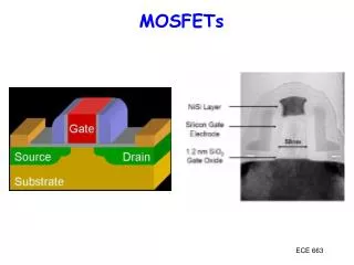
nMOS Transistor • Four terminals: gate, source, drain, body • Gate – oxide – body stack looks like a capacitor • Gate and body are conductors • SiO2 (oxide) is a very good insulator • Called metal – oxide – semiconductor (MOS) capacitor
nMOS Operation • Body is commonly tied to ground (0 V) • When the gate is at a low voltage: • P-type body is at low voltage • Source-body and drain-body diodes are OFF • No current flows, transistor is OFF
nMOS Operation Cont. • When the gate is at a high voltage: • Positive charge on gate of MOS capacitor • Negative charge attracted to body • Inverts a channel under gate to n-type • Now current can flow through n-type silicon from source through channel to drain, transistor is ON 0: Introduction
pMOS Transistor • Similar, but doping and voltages reversed • Body tied to high voltage (VDD) • Gate low: transistor ON • Gate high: transistor OFF • Bubble indicates inverted behavior
Power Supply Voltage • GND = 0 V • In 1980’s, VDD = 5V • VDD has decreased in modern processes due to scaling • High VDD would damage modern tiny transistors • Lower VDD saves power (Dynamic power is propotional to C.VDD2.f.a) • VDD = 3.3, 2.5, 1.8, 1.5, 1.2, 1.0, …
Transistors as Switches • We can view MOS transistors as electrically controlled switches • Voltage at gate controls path from source to drain
CMOS NAND Gate 0: Introduction
Objective of the Lecture • Design of Logics in CMOS • Why to Study Fabrication? • Flow Diagram. • Fabrication Process Flow:Basic Steps
3-input NAND Gate • Y pulls low if ALL inputs are 1 • Y pulls high if ANY input is 0
3-input NAND Gate • Y pulls low if ALL inputs are 1 • Y pulls high if ANY input is 0
Complementary CMOS • Complementary CMOS logic gates • nMOS pull-down network • pMOS pull-up network • a.k.a. static CMOS
Series and Parallel • nMOS: 1 = ON • pMOS: 0 = ON • Series: both must be ON • Parallel: either can be ON
Conduction Complement • Complementary CMOS gates always produce 0 or 1 • Ex: NAND gate • Series nMOS: Y=0 when both inputs are 1 • Thus Y=1 when either input is 0 • Requires parallel pMOS • Rule of Conduction Complements • Pull-up network is complement of pull-down • Parallel -> series, series -> parallel
Compound Gates • Compound gates can do any inverting function • Ex:
Objective of the Lecture • Design of Logics in CMOS • Why to Study Fabrication? • Flow Diagram. • Fabrication Process Flow:Basic Steps
Why to study Fabrication? • Strong link between Fabrication Process , the circuit design procedure and the performance of resulting chip • The circuit designer must have clear understanding of the roles of various MASKs used in the fabrication procedure and How this MASKs define various feature of the devices on a Chip • To know to create effective design. • To optimize the circuit with respect to various manufacturing parameters.
Well • Requires to build both pMOS and nMOS on single wafer. • To accommodate both pMOS and nMOS devices, special regions must be created in which the semiconductor type is oppossite of the substrate type. • Also Known as Tubs. • Twin-tubs
Objective of the Lecture • Design of Logics in CMOS • Why to Study Fabrication? • Flow Diagram. • Fabrication Process Flow:Basic Steps
Flow Diagram Create n-Well regions and Channel Stops region Grow Field Oxide and Gate Oxide Deposite and pattern Polysilcon Layer Implant sources, drain regions and substrate contacts Create contact Windows, deposit and pattern metal layer
Objective of the Lecture • Design of Logics in CMOS • Why to Study Fabrication? • Flow Diagram. • Fabrication Process Flow:Basic Steps
Fabrication Procedure Flow: Basic Steps • Masks: Each Processing steps in the fabrication procedure requires to define certain area on the chip. This is known as Masks. • Chips are specified with set of masks • Minimum dimensions of masks determine transistor size (and hence speed, cost, and power) • Feature size f = distance between source and drain • Set by minimum width of polysilicon • Feature size improves 30% every 3 years or so • Normalize for feature size when describing design rules • The ICs are viewed as a set of pattern layers of doped Silicon, Polysilicon, Metal and Insulating Silicon Dioxide. • A layer mut be Patterned before the next layer of material is applied on the chip.
Inverter Cross-section • Typically use p-type substrate for nMOS transistors • Requires n-well for body of pMOS transistors
Inverter Cross-section with Well and Substrate taps • Typically use p-type substrate for nMOS transistors • Requires n-well for body of pMOS transistors • Substrate must be tied to GND and n-well to VDD • Metal to lightly-doped semiconductor forms poor connection • Use heavily doped well and substrate contacts / taps
Inverter Mask Set • Transistors and wires are defined by masks • Cross-section taken along dashed line
Detailed Mask Views • Six masks • n-well • Polysilicon • n+ diffusion • p+ diffusion • Contact • Metal
Chrome Pattern Pellicle Quartz Substrate Pattern Preparation